Download
1 / 5
50 likes | 183 Views
High Resolution Energy Loss Spectroscopy of “Sheet” Plasmons. Roy F. Willis, Department of Physics, The Pennsylvania State University University Park, PA 16802.

E N D
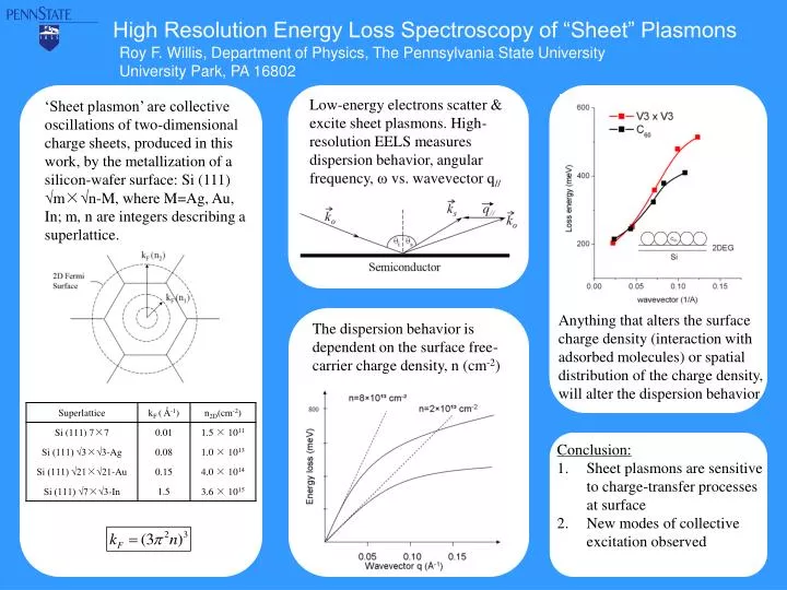
High Resolution Energy Loss Spectroscopy of “Sheet” Plasmons Roy F. Willis, Department of Physics, The Pennsylvania State University University Park, PA 16802 Low-energy electrons scatter & excite sheet plasmons. High-resolution EELS measures dispersion behavior, angular frequency, ω vs. wavevector q// ‘Sheet plasmon’ are collective oscillations of two-dimensional charge sheets, produced in this work, by the metallization of a silicon-wafer surface: Si (111) √m×√n-M, where M=Ag, Au, In; m, n are integers describing a superlattice. Anything that alters the surface charge density (interaction with adsorbed molecules) or spatial distribution of the charge density, will alter the dispersion behavior The dispersion behavior is dependent on the surface free-carrier charge density, n (cm-2) • Conclusion: • Sheet plasmons are sensitive to charge-transfer processes at surface • New modes of collective excitation observed
kF (n2) C60 2DEG 2D Fermi Surface Si kF (n1)
ks n=8×10¹³ cm-² ko ko n=2×10¹³ cm-2 800 Energy loss (meV) 0.05 0.10 0.15 Wavevector q (Å-1) q// θi θs Semiconductor
Surface plasmon polariton of wavevector q=2π/λ; (a) surface change density distribution; (b) electric field lines Fig 1 λ (a) wavevector q (b)
5.4 x 1013 cm-2 3.4 x 1013 cm-2 3.0 x 1013 cm-2