Download
1 / 24
280 likes | 497 Views
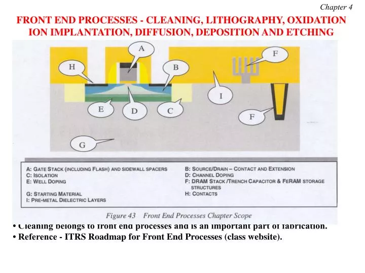
Chapter 4. FRONT END PROCESSES - CLEANING, LITHOGRAPHY, OXIDATION ION IMPLANTATION, DIFFUSION, DEPOSITION AND ETCHING. • Cleaning belongs to front end processes and is an important part of fabrication. • Reference - ITRS Roadmap for Front End Processes (class website).

E N D
Chapter 4 FRONT END PROCESSES - CLEANING, LITHOGRAPHY, OXIDATION ION IMPLANTATION, DIFFUSION, DEPOSITION AND ETCHING • Cleaning belongs to front end processes and is an important part of fabrication. • Reference - ITRS Roadmap for Front End Processes (class website).
Semiconductor Manufacturing Clean Rooms, Wafer Cleaning and Gettering Importance of unwanted impurities increases with shrinking geometries of devices. 75% of the yield loss is due to defects caused by particles (1/2 of the min feature size) Crystal originated (45-150nm) particles (COP) ~1,000Å=void with SiOx -> affect GOI -> anneal in H2 -> oxide decomposes and surface reconstructs! & oxide precipitates from deep depth in Si. Yield -> 90% at the end -> 99% @ each step
Historical Development and Basic Concepts Contaminants and their role in devices (various elements, various films) Particles cause defects ! ! QM Life time killers ! ! Poly-Si, silicides Na+, Ka+ XOX ~10nm QM≈ 6.5x1011cm-2, VTN=0.1V (equivalent to 6.7*1017 cm-3 or 10 ppm contaminations)
SEMICONDUCTOR MANUFACTURING - CLEAN ROOMS, WAFER CLEANING AND GETTERING • Modern IC factories employ a three tiered approach to controlling unwanted impurities: 1. clean factories 2. wafer cleaning 3. gettering Up till 2018 2003 ITRS Front End processes - see class website • Contaminants may consist of particles, organic films (photoresist), heavy metals or alkali ions.
Dynamic Random Access Memory Vth~107cm/sec write, read ~10-15cm-2 Deep-level traps (Cu, Fe, Au etc.) Pile up at the surface where the devices are located. Leakage currents discharge the capacitor (mechanism SRH) refresh the charge storage (time ~ a few msec) Lifetime must be > ~ 25 µsec Use gettering to keep Nt <1012 cm-3(Nt< ppb) -> G≈100µsec
Role of Surface Cleaning in Processing Oxide thickness [Å] Residual contaminants, layers affect kinetics of processes. Surface effects are very important (MORE) in scaled down devices
Level 1 Contamination Reduction: Clean Factories • Air quality is measured by the “class” of the facility. Factory environment is cleaned by: • Hepa filters and recirculation for the air, • “Bunny suits” for workers. • Filtration of chemicals and gases. • Manufacturing protocols. (Photo courtesy of Stanford Nanofabrication Facility.)
Level 1 Contamination Reduction: Clean Factories Ex. Class 100 -> 5 particles/cm, >0.1 µm in 1hr. Small particles remain in air (long) coagulate large ones precipitate quickly and deposit on surfaces by (small) Brownian motion and gravitational sedimentation (larger). Class 1-100,000 mean number of particles, greater than 0.5 m, in a foot of air Use local clean rooms from Particles ---> people , machines, supplies suits Material filters Chemicals, water (use DI)
Level 2 Contamination Reduction: Wafer Cleaning Front End Process Back End Oxygen plasma H2S04 +H2O2 Oxygen plasma Organic strippers (do not attack metals) Good clean for high T steps Low T - less critical Oxidizes organic films Oxidizes Si and complexes metals 5 H20 + H2O2 + NH4OH SC1 Small content reduces Si etch (0.05%) 6H2O : H2O2 : HCl SC2 Removes alkali ions & cations Al3+, Fe3+, Mg3+ (insoluble in NH4OH - SC1) Ultrasonic and now megasonic cleaning for particulates removal (20-50 kHz) DI water is necessary: H2O<-> H++OH- [H+]=[OH-]=6x10-13cm-3 Diffusivity of: H+≈9.3x10⁻⁵cm2s-1 -> µH+=qD/kT=3.59cm2V-1s-1 of : OH-≈5.3x10⁻⁵cm2s-1 -> µOH-=qD/kT=2.04cm2V-1s-1
Level 2 Contamination Reduction: Wafer Cleaning with all contaminants -> H passivation (or F!) NH4OH small -> reduce surface roughness • RCA clean is “standard process” used to remove organics, heavy metals and alkali ions. • Ultrasonic agitation is used to dislodge particles. Not removed by SC1 HF dip added to remove oxide
Level 3 Contamination Reduction: Gettering • Gettering is used to remove metal ions and alkali ions from device active regions. • For the alkali ions, gettering generally uses dielectric layers on the topside (PSG or barrier Si3N4 layers). • For metal ions, gettering generally uses traps on the wafer backside or in the wafer bulk. • Backside = extrinsic gettering. Bulk = intrinsic gettering.
Gettering Concepts: contaminants freed diffuse become trapped PSG (for alkali ions Na+, K+ and metals) affects E fields (dipoles in PSG) and absorbs water leading to Al corrosion (negative effects) or Si3N4 Fast Diffusion of Various Impurities Closer to devices than to a backside layer -> high efficiency metals Metal contaminants will be trapped by dislocations and SF (decorate) and far away from ICs
• Heavy metal gettering relies on: • Metals diffusing very rapidly in silicon. • Metals segregating to “trap” sites.
Intrinsic Gettering Oxygen ~ 1018 cm-3;15-20 ppm Oi>20ppm -> too much precipitation-> strength decreases and warpage increases Oi<10ppm -> no precipitation-> no gettering >> Ddopants but D0<< Dmetals denuded zone = oxygen free; thickness several tens of µm Slow ramp 50-100 µm in size 1-3 nm min size of nuclei, concentrations ≈ 1011cm-3 • “Trap” sites can be created by SiO2 precipitates (intrinsic gettering), or by backside damage (extrinsic gettering). • In intrinsic gettering, CZ silicon is used and SiO2 precipitates are formed in the wafer bulk through temperature cycling at the start of the process. SiO2 precipitates (white dots) in bulk of wafer.
Intrinsic Gettering Due to Oxide Precipitates Precipitates (size) grow @ high T Density of nucleation sites grow @ low T The largest & the most dense defects -> the most efficient gettering
Measurement Methods Clean factories = particle control. Detect concentrations < 10/wafer of particles smaller than 0.1 µm • Unpatterened wafers (blank) • Count particles in microscope • Laser scanning systems -> maps of particles down to ≈ 0.2 µm • Patterned wafers • Optical system compares a die with a “known good reference” die (adjacent die, chip design - its appearance) • Image processing identifies defects (SEM) • Test structure (not in high volume manufacturing)
Test Structures Trapped charge QT VTH change Dielectric breakdown due to particles, metals etc. Models relate type of defects (typical for processes) with yields Water – measure water resistivity Deionized Water r=18.5 M H2O H+ + OH-
Monitoring the Wafer Cleaning Efficiency Concentrations of impurities determined by surface analysis works with SEM He+ 1-3 MeV O+ or Cs+ sputtering and mass analyses • Excite • Identify (unique atomic signature) • Count concentrations emitted Primary beam – e - good lateral resolution Detected beam – e – good depth resolution and surface sensitivity X-ray poor depth resolution and poor surface sensitivity ions (SIMS) excellent ions (RBS) good depth resolution, reasonable sensitivity (0.1 atomic%)
Electrons in Analytical Methods (as in SEM) Inelastic collisions with target electrons, which are then emitted from the solid Elastic collision of incoming electrons with atoms (reflected back) ~ the same energy as for the incoming electrons ~ 5 eV
Analytical Techniques • If X-Ray is at the input: • el. Emitted= X-ray Photoelectron Spectroscopy (XPS) • X-ray emitted= X-ray Fluorescence (XRF) • XPS usually more dominant for lighter elements, XRF for heavier This scheme is for lighter elements (Z=33 as is crossover b/w Auger and X-Ray Several keV 3 3 Several keV The core electron energy levels 2 2 1 kicked out a core electron 1 Electron Microprobe X-Ray Electron Spectroscopy Auger El. Spectroscopy
Monitoring of Gettering Through Device Properties and Dielectric p – n leakage, refresh time DRAM junction and dielectric breakdown, b of n-p-n emission<-> capture Material properties : G(>>R) in the bulk and on the surface Photoconductive Decay Measurements ∆n=goptG • Carriers are generated due to light • Decrease resistivity • Recombine
Carrier Generation Lifetime = = inversion + DL Deep Depletion - Return to Inversion via Carrier Generation (measure tG) and surface recombination (s) Zerbst technique: s=f(NST, ) if plotted vs. (Cmin/C)-1 =Capture cross section
Lifetime Measurements: Open Circuit Voltage Decay t=0 ≈0.7V Diode switched from ON VD when carriers recombine off for t>4 Measurements include surface and bulk recombination Use also DLTS: identifies traps (Et) and concentrations Thermal or photoexcitation processes in voltage modulable space-charge region (Schottky Diode, p-n junction, MOS Capacitor) Measured: capacitance, currents or conductance
Excess Carrier Concentrations Decays: minority carriers Mobility of minority carriers Experiment to calculate the diffusion constant Dp, (n) for minority carriers (dpn) -> µp, (n) Drift&diffusion diffusion Dx=DtL/td Pulse oscilloscope screen Drift: vd=L/td µp=vd/E Mobility of minority carriers vd-> µ