Download
1 / 34
380 likes | 531 Views
Semiconductors and Carrier Concentrations. Reading Assignment : Pierret Chap 1, Chap 2. Instructor : Prof. Dr. Ir. Djoko Hartanto, M.Sc. : Arief Udhiarto, M.T Source : U.C. Berkeley. Bohr Model. Silicon Atom. 1s, 2s, 2p orbitals filled by 10 electrons

E N D
Semiconductorsand Carrier Concentrations Reading Assignment : Pierret Chap 1, Chap 2 Instructor : Prof. Dr. Ir. Djoko Hartanto, M.Sc. : Arief Udhiarto, M.T Source :U.C. Berkeley
Bohr Model Electrical Engineering Department University of Indonesia
Silicon Atom • 1s, 2s, 2p orbitals filled by 10 electrons • 3s, 3p orbitals filled by 4 electrons 4 nearest neighbors unit cell length = 5.43Å 5 × 10²² atoms/cm3 The Si Atom The Si Crystal “diamond cubic ” structure Electrical Engineering Department University of Indonesia
Conduction Band and Valence Band Electron Potential Energy Electrical Engineering Department University of Indonesia
The Simplified Energy Band Diagram Electrical Engineering Department University of Indonesia
Semiconductors, Insulators, and Conductors • Totally filled band and totally empty bands do not allow current flow. (just as there is no motion of liquid in a totally filled or totally empty bottle • Metal conduction band is half-filled • Semiconductors have lower Eg’s than insulators and can be doped Electrical Engineering Department University of Indonesia
Compound Semiconductors • “Zincblende Structure” • III-V compound semiconductors : GaAs, GaP, GaN, etc. • “important for optoelectronics and high speed ICs” Electrical Engineering Department University of Indonesia
Density of States Electrical Engineering Department University of Indonesia
Density of States at Conduction Band:The Greek Theater Analogy Electrical Engineering Department University of Indonesia
Concept of a “hole” An unoccupied electronic state in the valence band is called a “hole” Treat as positively charge mobile particle in the semiconductors Electrical Engineering Department University of Indonesia
Bond Model of Electrons and Holes Electrical Engineering Department University of Indonesia
N-type (Arsenic) Doped Silicon and Its Donor Energy Band Si Si Si Extra Si As Si Si Si Si - Conducting band, Ec Ed ~ 0.05 eV Electron Eg = 1.1 eV Valence band, Ev Electrical Engineering Department University of Indonesia
P-type (Boron) Doped Silicon and Its Acceptor Energy Band Conducting band, Ec Si Si Si Hole Eg = 1.1 eV Si B Si Ea ~ 0.05 eV Si Si Si - Valence band, Ev Electron Electrical Engineering Department University of Indonesia
Electrons and Holes Electrical Engineering Department University of Indonesia
The Fermi-Dirac Distribution (Fermi Function) Probability of available states at energy E being occupied f(E) = 1/ [1+ exp (E- Ef) /kT] where Ef is the Fermi energy and k = Boltzmann constant=8.617 .10-5 eV/K Electrical Engineering Department University of Indonesia
Properties of the Fermi-Dirac Distribution (1) f(E) .exp [- (E- Ef) /kT] for (E- Ef) >3kT This approximation is called Boltzmann approximation (2) Probability of available states at energy E NOT being occupied 1- f(E) = 1/ [1+ exp (Ef -E) /kT] Electrical Engineering Department University of Indonesia
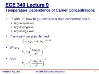
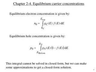
Equilibrium Carrier Concentrations • Integrate n(E) over all the energies in the conduction band to obtain • By using Boltzmann approximation, and extending the integration limit to ~, we obtain Electrical Engineering Department University of Indonesia
Integrate p(E) over all energies in the valance band to optain p • By using Boltzmann approximation, and extending the integration limit to ~, we obtain Electrical Engineering Department University of Indonesia
Carrier Concentrations of Pure (“intrinsic”) Semiconductor • For each electron in the conduction band (i.e. an occupied state in CB), there must be a hole in the valence band (i.e. unoccupied state in VB) Therefore n= pwhich can defined as an intrinsic concentration ni Electrical Engineering Department University of Indonesia
Intrinsic Carrier Concentration versus Temperature Electrical Engineering Department University of Indonesia
Fermi Energy (Ei) of Intrinsic Semiconductor Electrical Engineering Department University of Indonesia
Physical Interpretation of NC and NV The average electron energy <E> of all electrons in conduction band is only 1.5kT above Ec ! We can treat all the available density of states in the conductor band as a single energy level exactly at EC, with an effective density of states of NC. The electron concentration can simply be calculated as NC * f(E=EC). Electrical Engineering Department University of Indonesia
Doping • By substituting a Si atom with a special impurity atom (Column V or Column III element), a conduction electron or hole is created. Dopant concentrations typically range from 1014 cm-3 to 1020 cm-3 Electrical Engineering Department University of Indonesia
Energy Band Description of Electrons and Holes Contributed by Donors and Acceptors Electrical Engineering Department University of Indonesia
Charge Neutrality Condition Electrical Engineering Department University of Indonesia
Charge-Carrier Concentrations n : electron concentration (cm-3) p : hole concentration (cm-3) N+D: ionized donor concentration (cm-3) ≡ND N-A: ionized acceptor concentration (cm-3) ≡NA (1) Charge neutrality condition:ND+p =NA+n (2) At thermal equilibrium, np =ni2 (“Law of Mass Action”) Electrical Engineering Department University of Indonesia
n-type and p-type Semiconductors Electrical Engineering Department University of Indonesia
Dependence of Fermi Level with Doping Concentration Electrical Engineering Department University of Indonesia
The Fermi Energy Ef for doped semiconductors can be determined from either one of the following relationships once n and p are known Electrical Engineering Department University of Indonesia