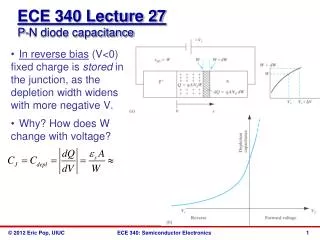
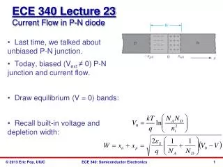
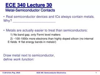
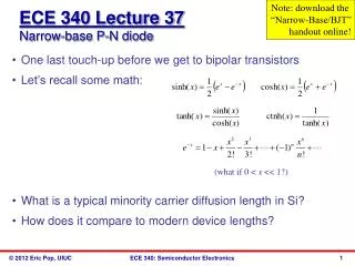
Download
1 / 16
180 likes | 457 Views
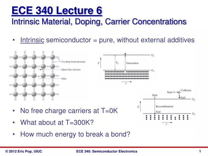
ECE 340 Lecture 6 Intrinsic Material, Doping, Carrier Concentrations. Intrinsic semiconductor = pure, without external additives No free charge carriers at T=0K What about at T=300K? How much energy to break a bond?.

E N D
ECE 340 Lecture 6Intrinsic Material, Doping, Carrier Concentrations • Intrinsic semiconductor = pure, without external additives • No free charge carriers at T=0K • What about at T=300K? • How much energy to break a bond?
How many electron-hole pairs (EHPs) are created when bonds are broken by thermal agitation? • In thermal equilibrium • generation = recombination • Simple probability: • Recombination driven by… • Generation intrinsically driven only by… • Hence the np product at thermal equilibrium:
At room temperature (T ~ 300 K) intrinsic concentrations: • ni ~ 2 x 10⁶ electrons and holes per cm3 in GaAs • ~ 1 x 1010 cm-3 in Si • ~ 2 x 10¹³ in Ge • What about the band gaps of these materials? • To get a sense of scale, how do these numbers: • compare with NA? • compare with number of Si atoms per cm3 (x4 valence electrons per atom)? • What if temperature is increased?
How to manipulate carrier concentrations • Doping = purposely introducing impurities into the crystal • Intrinsic material = pure, undoped. Extrinsic = doped. • Donors and acceptors… of what? • Ex: compare # of valence electrons (e.g. 5 for As) with number of electrons of the atom it replaces (e.g. 4 for Si)
Arsenic (As) dopant in Si: 4 electrons used up for bonding with neighbors. But, how loosely bound is that 5th electron that As brought into the Si lattice? • Approximate binding energy using Niels Bohr’s model: • The real numbers of donors and acceptors in Si: • (note: binding energy = ionization energy) be careful with choice of m* and K = 4πϵrϵ0
Where are the donor and acceptor levels on the band diagram model? • Recall: thermal agitation energy ~ 3/2 kBT
Extrinsic (doped) material: • n-type semiconductor if… • p-type semiconductor if… • Ex: what are the electron & hole concentrations in a Si wafer doped with 1015 cm-3 As atoms (at room T). Is this n- or p-type Si? • How much has the resistivity changed from intrinsic Si?
Summary: • Band gap energy (EG) is energy required to free an electron from a covalent bond • EG = 1.1 eV for Si at 300 K • Insulators have “large” EG, semiconductors have “small” EG • Dopants in Si: • Substitute pre-existing Si atoms on lattice sites • Group-V elements are donors, contribute conduction electrons • Group-III elements are acceptors, contribute holes • Low ionization energy (~50 meV) all ionized at room T • Useful dopant concentrations in Si range from 1015 to 1020 cm-3
ECE 340 Lectures 7-8Doping, Fermi Level, Density of States • How to calculate electron (and hole) densities for: • Any temperature • Any doping concentration • Any energy level • Recall that in thermal equilibrium: np = ni2 • What if I turn the light on? (qualitatively)
We are (typically) dealing with large concentrations, not individual electrons we need a statistical treatment of these electron (or hole) populations • Two key concepts needed to “count” populations: • The probability of finding electrons (or holes) in a state • The number (i.e. density) of states available • Recall that electrons (and holes) obey the Pauli exclusion principle, i.e. electrons are fermions • So are neutrons, protons (all spin = _____) • But photons and phonons (vibrations) are bosons
1) Fermi-Dirac probability function for electrons & holes ≈ the probability of finding a spectator in a seat as you go up from the bottom row of a stadium • What does this look like? • What is the meaning of the Fermi level, EF? T=0 T=300 K f (E) T=1000 K
2) Density of states in Si conduction & valence band • Counting states (i.e. “stadium seats per row”) in App. IV: • Most important feature is ~E1/2 (more states at higher E) • What is E with respect to? Any states in the band gap? • What is m* here? • Bonus question: what about in 1-D and 2-D devices?
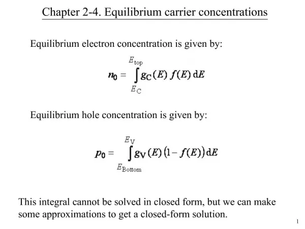
So how do we calculate electron & hole concentrations knowing the density of states and probability of occupation? • This is the density of electrons in the C-band. What about holes in the V-band? • This is usually a tough numerical integral, but we can approximate it if EF is well inside the band gap where
Where is EF in intrinsic material? • What happens with EF when we start doping the material?
We can write similarly for holes: • And so the product: • Is there an easier way to write these? • Recall if the material is intrinsic, EF = Ei = where? • EC – Ei = EG/2 • Write ni with NC and NV as above • But we know ni ~ ______ so it’s easier to re-write: (is the product as it should be?)
Sample problem: Si doped with 1016 Boron atoms per cm3. What are the electron & hole concentrations at room T? (assume lights off.) Is this n- or p-type material? Where is the Fermi level EF?