Download

1 / 44
530 likes | 1.01k Views
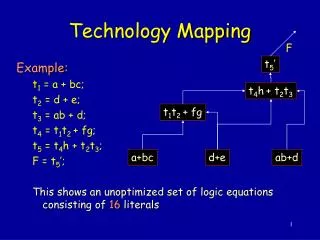
Technology Mapping. Technology Mapping. Perform the final gate selection from a particular library Two basic approaches 1. ruled based technique 2. graph covering technique. Technology Mapping. Create subject graph

E N D
Technology Mapping • Perform the final gate selection from a particular library • Two basic approaches 1. ruled based technique 2. graph covering technique
Technology Mapping • Create subject graph • transform a given graph to a subject graph using only gates in the base function
Technology Mapping • choice of base function • functionally complete ex: AND-OR-NOT NOR-NOT NAND-NOT • the decision of base function influences the number of patterns needed to represent the library ex: to represent a cell f=(ab+cd)’ if base function (NAND,NOR,INV) - 3 NAND gate, 1 INV - 3 NOR gate, 4 INV - ......... if base function (NAND,INV) - one pattern only
Technology Mapping • the granularity of the base function affects the optimization potential ex: f=abcd+efgh+ijkl+mnop 4-input nand gates => one mapping 2-input nand gates => 18 mappings A fine resolution base-function allows for more cover and thus better quality
Graph Covering (Mapping) • DAG covering is NP-hard • Heuristic to solve the problem (tree covering) 1. Partition the subject graph into trees 2. Cover each tree optimally (Dynamic Programming)
Graph Covering (Mapping) Step 2: Library Subject graph Bottom-up For each nodes . find all matching which rooted at v . select the best matching which has the least cost inv(2) nand2(3) AOI21(4)
Graph Covering (Mapping) Step 1: (a) Graph => tree • weak points: • loss of global view due to the step of • partition into trees • cover cross bounding is not allowed • xor type gate can not be explored
Graph Covering (Mapping) (b) • only primary output is selected as root • the mapping starts at a primary output • mapping continues until either a primary input is encountered or until another internal node that already mapped is encounter which is an output of a cell • select the most critical output first (mapping without interruption)
Technology Mapping Minimizing Area under Delay Constraint • Minimize area subject to constraints on signals arrival times at the output. Two steps: (1) Compute delay function (arrival time-area trade off curve) at all nodes bottom up (2) Generate the mapping solution based on the delay function and required time at each nodes top down
Technology Mapping Minimizing Area under Delay Constraint Step 1: (post-order traversal) 1. At each node, compute the area as a function of arrival time. Delay function computation: Let Gate G (a mapping) have inputs A,B a) select a point from delay function of one input (A) b) look for a point on the delay function of the other node(B) with “less delay” & ”minimum area” c) combine these two points arrival time(G) = arrival time(A) + delay(y) area(G) = area(A) + area(B) + gate(g)
c’ b’ area d’ a’ gate delay = 1/2 gate area = 1/2 delay D c e b area C d a delay B A Generating the delay curve for a given match
a d area b /* point c becomes inferior point */. e delay merged delay curve due to g1 & g2 d a area area e b c C g1 g2 delay delay delay curve due to match g1 B A Lower bound merging of delay curves
Technology Mapping Minimizing Area under Delay Constraint 2. Lower bound merge process • delete inferior points inferior point p* = (t*,n*) if there exists a point p = (t,a), t > t* and a* > a Step 2: Timing recalculation (shift the delay curve) Step 3: According to the delay function and required time, select mappings. (preorder traversal)
Technology Mapping for FPGA Interconnection Resources Logic Block I/O Cell Fig.1.1- A Conceptual FPGA. FPGA : Field Programmable Gate Arrays
Technology Mapping for FPGA X Inputs A B C D Look-up Table Y Outputs s D Q R Note: = User-programmed Multiplexor XC2000 CLB
Technology Mapping for FPGA e f c (a+b)’(c’e+cf) +(a+b)(d’g+dh) g h d a b Figure 3.19- Act-1 Logic Block.
Technology Mapping for FPGA Traditional Logic Synthesis Tools: Logic description literal counts as criterion f1=x1 | x2 | x3 | x4 | x5 | x6 f2= x1 x2’ x3’ x4’ x5’| x1’ x2 x3’ x4’ x5’ ...| x1 x2 x3 x4 x5 Decomposition process Technology mapping gate library (For a 5-input RAM cell, 22 gates are needed.) 5 A mapped logic description ( a general graph)
Technology Mapping for FPGA Some Features of the FPGA: (1) Configurable function units and interconnections. (2) Function units are implemented using lookup tables. ( Number of literals are not so important any more Ex: f1 = abcdef f2 = abcde + b’d + ab’c + bcd’) (3) Restricted interconnections.
F G g f y x a b c d Technology Mapping For FPGA 1. Decomposition k=3
Technology Mapping For FPGA 2. Covering k=5 a) With forced merge, 2 LUTs b) Without forced merge, 3 LUTs
Technology Mapping For FPGA a) Without replicated logic, 3 LUTs b) With replicated logic, 2 LUTs
f MIS-PGA 1. SIS standard script optimization 2. Decomposition so that each intermediate node with input less that K(input constraint of a logic cell) • Roth-Karp decomposition • partition • kernel extraction f = ciki+ri cost(ki) = • and-or decomposition f = ab+bc+cd => g = bc+cd f = ab+g
Unate Covering A covering problem where the coefficients of the matix is 0 or 1 and row i is covered if column Aj is selected and Aij = 1 . (ie. select a set of Aiso that all row ais are covered) A1 A2 A3 a1 1 1 a2 1 1 a3 1 1 c = { A1, A3 } or c = { A2, A3 }
Binate Covering A covering problem where the coefficient of the matrix can be -1, 0, 1 and row ai is covered if column Aj is selected and aij=1 or Aj is NOT selected and aij=-1. A1 A2 A3 a1 1 1 a2 1 1 a3 1 1 a4 -1 c = { A1,A3 }
Covering • Covering • find all supernode(i) for each node i • Supernode(i) : a cluster that rooted at i and some nodes in the transitive fan-in of i. The constraint is that it has a maximum of m inputs. supernode
Covering Use maxflow to find supernodes : Because we are going to find node cut set, For each node i: Different construction of network will result in different cut-set. 1
Binate Covering S5 n6 S1 n1 n7 n2 n3 S2 S4 n4 n5 S3 Covering constraint: Every intermediate node should be included in at least one selected FPGA node Implication constraint: If a supernode is chosen, each input to the supernode must be chosen. Output constraint: For every primary output, one supernode rooted at the outputs should be selected.
Example S5 n6 S1 n1 n7 n2 n3 S2 S4 n4 n5 S3
Binate Covering (一) Covering constraint For every intermediate node, we construct a row. The column index is the node of supernode If ni intermediate node is covered by supernode Sj, then Mij = 1 Example : S1 S2 S3 S4 n1 1 n2 1 n3 1 1 n4 1
Binate Covering (二) Implication constraint: For every input j to the supernode Si one row has to be added. entry under Mj Si = -1 and all supernode Sja has j as output Mj Sja = 1
Example Si ...... Sj1....Sj2 j1 -1 1 j2 -1 1 Si j2 j1 Si... Sja.. Sjb... j -1 1 1 Si j Sja Sjb
Binate Covering (三) Output constraint: For every primary output, we should create a row so that one supernode rooted at the output will be selected. primary output S1 S2 Si ..... Sj O1 1 1
Optimal Technology Mapping for Delay Optimization – Flow -Map • Unit delay model (one LUT = one unit delay) • Minimize the level of output node • Two-step algorithm of flow-map • Labeling phase (from input to output) • Mapping phase (from output to input)
Flow –Map : Two-Step Algorithm • Labeling phase (from input to output) • Mapping phase (from output to input)
The Minimum Level of an LUT Rooted at t The partial network The highest 3-feasible cut Determining l(t)
No Known Polynomial Algorithm for Minimum Height K-feasible Cut + 1 The highest 3-feasible cut
Transformation of Graph • t is the node to be processed: • Let p be the maximum label of the nodes in Nt • Collapse all the nodes in Nt with level = p, together with t, into the new sink • Node cut transformation • Check if there is a k-feasible cut • If yes, node t can be packed with the nodes in and l(t) = p • If no, {{Nt – t}, {t}} is such a cut and the l(t) = p + 1
Flow –Map : Two-Step Algorithm • Labeling phase (from input to output) • Mapping phase (from output to input)
Mapping phase • Let L contain all PO nodes. Process nodes in L one by one. • For a node v in L, is the minimum height K-feasible cut that computed in the labeling phase. Generate an LUT for it. • Put all inputs of this LUT to L. • 4. Continue steps 2 and 3 until L becomes empty