Download
1 / 19
260 likes | 783 Views
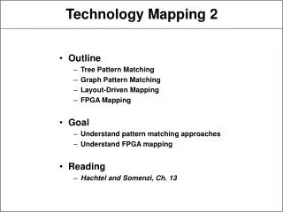
Outline What is Technology Mapping? Rule-Based Mapping Tree Pattern Matching Goal Understand technology mapping Understand mapping algorithms Understand mapping issues. Technology Mapping. Map optimized logic to primitive cell library Library capabilities function cell size

E N D
Outline What is Technology Mapping? Rule-Based Mapping Tree Pattern Matching Goal Understand technology mapping Understand mapping algorithms Understand mapping issues Technology Mapping
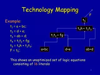
Map optimized logic to primitive cell library Library capabilities function cell size cell performance Library restrictions fan-in fan-out Goal delay area power etc. What is Technology Mapping? • Cell AOI33 • - area 3248 • - delay 0.8 • - power 0.08
Custom cells synthesize functions as needed e.g. complementary, domino, or CVSL CMOS Standard cells library of fixed functions use as needed e.g. 3-input AND-OR Gate arrays fixed population of gates and gate types must fit design into available gates FPGAs programmable function blocks e.g. all functions of 4 inputs Cell Libraries a b ab a b
Mechanically transform function to custom cell complementary CMOS - cell is guaranteed to work but it might be slow - e.g. 20-input NAND gate avoid problems by limiting functions in synthesis process limit fan-in, fan-out of functions chop up large functions Apply electrical rules size transistors to meet timing goals speed up longest paths in circuit rules are specific to cell technology Custom Cell Synthesis ABCDEF => (ABC)(DEF) A+B+C+D => (A+B)+(C+D) a b ab a in series, so make fatter speeds up 1->0 transition b
Library-based transformations rules encode library capabilities and restrictions transformations improve area, delay, power, etc. similar to synthesis via local optimization SOCRATES circuit optimizer lookahead several rules test all applicable rules avoid local minima Problems rules are not guaranteed to find optimum rules may not be complete X X Rule-Based Cell Matching
Rule-Based Matching Algorithm TryRule3(circuit, rule) { scan circuit for rule match if match, compute cost recurse twice more on all rules return minimum cost } do { mincost = cost; for (i = 0; i < MAXRULES; i++) { cost = TryRule3(circuit, rule[i]); if (cost < mincost) { mincost = cost; minrule = rule[i]; } if (minrule != NULL) cost = ApplyRule(circuit, minrule); } until no rules apply Complexity (CN)3 for C circuit elements and N rules
Logic Equation Representation directed acyclic graphs (DAGs) 2-input NANDs and inverters in MIS representation is not unique Library Cell Representation represent cells as DAGs 2-input NANDs and inverters in MIS all decompositions of a cell function ~N! possibilities for N inputs cell cost (area, delay, power) F = abcd F F F d b a c d b a b a c c d Graph Covering NOT F NAND a b c d • • •
Algorithm minimum-cost cover of equation DAGs with library DAGs NP-complete (Bruno and Sethi 1975) same problem as compiler code generation Approaches search from primary inputs search from primary outputs try largest cell DAGs first usually smallest area not always fastest similar to “maximal munching” in code generation avoid local minima lookahead several random starting points F = abcd Graph Covering F a b c d F a b c d
Partition circuit DAGs into trees split at fan-out nodes make only outputs roots of trees perform splitting incrementally when searching that tree stop at already-mapped nodes Algorithm find optimal mapping for each output tree use recursive graph isomorphism tree matching match all cells at root (output) find optimum mapping for each subtree (cell input) cost is cell plus cost of mappings of cell inputs top-down traversal to record cells exponential time in worst case Tree Pattern Matching a c b a a b c b look at top input to NAND
Tree Pattern Matching OptimalTree(tree) { mincost = INF; for all cells if (cell matches at tree.root) { cost = cell.cost; for all cell inputs cost += OptimalTree(cell.input[i]); if (cost < mincost) { mincost = cost; keep tree mapping; } } return(mincost); } for each output { outputcost = OptimalTree(output); scan top-down to get cell mapping; } cost = 5+2+2+5+2+2 = 18 cost = 4+4 = 8
Inject inverter pairs at gate outputs increases possible matches add fake inverter pair cell to library removes remaining inverter pairs from circuit Tree Pattern Matching without inverters with inverters
Tree matching is fast simple DFS of circuit and cell trees Still many tree representations for a function Might miss common subexpressions if cell matching does not line up with fan-out nodes stop by treating fan-outs as cell outputs Tree Matching Issues a b a a b c b c c b b c d d c d 2-input ANDs cost: 15 xistors 3-input ANDs cost: 16 xistors
Match subgraphs, not trees avoid breaking graph into forest of trees match more gate types XOR, MUX multiple-output gates Algorithm find all circuit subgraph to cell graph matchings generate DFS traversal of each cell graph from outputs O(C*N) for C circuit nodes, N total cell library nodes cover graph with minimum-cost cell graphs matrix with row for each circuit node, column for each cell, 1 if cell matches circuit, 0 otherwise find least-cost maximum independent set of rows branch-and-bound search algorithm bound is least-cost rows found so far exponential in worst case Graph Pattern Matching
boolean CellMatch(x, y) if (y.gatetype != x.gatetype) return(0); i = y.firstchild; j = x.firstchild; while (i != NULL && j != NULL) if (!CellMatch(i,j)) return(0); i = y.nextchild; j = x.nextchild; if (j == NULL) return(1); else return(0); for each node i in circuit graph for each cell j in library graphs if (CellMatch(i,j)) match[i][j] = 1 find least-cost maximum set of independent rows in match array Graph Matching Algorithm
Minimum-Cost Graph Cover 2 3 XOR2 INV NOR2 NAND2 Cost 14 2 4 4 a 0 0 1 0 b 1 0 0 1 c 0 0 0 1 d 0 1 0 0 e 0 0 0 1 f 0 0 0 1 4 1 5 6 XOR Cell DFS d c e a b f first solution: a, b, c, d, e bound = 4 + 4 + 4 + 2 + 4 = 22 least-cost solution: a, b, d cost = 4 + 14 + 2 = 20 NOR2 at a XOR2 at b INV at d Circuit DFS a - fails at 1 b - match at 1 c - fails at 2 d - fails at 1 e - fails at 2 f - fails at 4 Maximum number of rows - cover most nodes in fewest cells Independent - cells do not overlap
Goal minimize chip area previous approaches focus on cell area ignore inter-cell routing example - high fan-in and fan-out minimizes cell area takes a lot of routing Solution estimate placement and routing during mapping simple, fast estimates incrementally update during mapping only mapping a few gates at a time Layout-Driven Mapping
Programmable logic blocks multiplexor-based (Actel) lookup table (Xilinx) Problem lookup table of K inputs implements possible functions K = 5 typically impractical to use library cell matching approach requires 4 billion variations for each cell pattern/tree/graph similar problem for mux-based FPGAs Solutions clique partitioning bin packing OBDD matching FPGA Technology Mapping
Xilinx RAM configurable logic blocks (CLB) RAM programmable wiring 2 functions of 4 variables 1 function of 5 variables implemented via table lookup RAM Actel fuse configurable logic elements fuse programmable wiring all 2 and 3-variable functions some 4-variable functions FPGAs CLB
Functions are implemented as MUX Interconnects are implemented as wire segment Interconnect connections are pass transistors Advantage: CMOS Disadvantage: slow Other issues: Need re-program each time power is on SRAM-based FPGA