Download
1 / 9

E N D
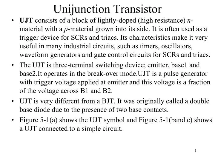
Unijunction Transistor • UJT consists of a block of lightly-doped (high resistance) n-material with a p-material grown into its side. It is often used as a trigger device for SCRs and triacs. Its characteristics make it very useful in many industrial circuits, such as timers, oscillators, waveform generators and gate control circuits for SCRs and triacs. • The UJT is three-terminal switching device; emitter, base1 and base2.It operates in the break-over mode.UJT is a pulse generator with trigger voltage applied at emitter and this voltage is a fraction of the voltage across B1 and B2. • UJT is very different from a BJT. It was originally called a double base diode due to the presence of two base contacts. • Figure 5-1(a) shows the UJT symbol and Figure 5-1(band c) shows a UJT connected to a simple circuit.
Figure 5–1(a) Schematic symbol and terminal names of a UJT. (b and c) A UJT connected into a simple circuit. This drawing shows the emitter current (IE), the emitter-to-base 1 voltage (VEBI), and the base 2-to-base 1 voltage (VB2B1). (c)
The base to base resistance RBB is the resistance of the device between terminals B2 and B1 when IE = 0, and can be considered as consisting of the resistors rB1 and rB2 in series. In equation form, • The magnitude of rB1 is typically from 5 to 12 kΩ. The resistance is fairly distributed between B1 and B2 when the emitter is open circuited (IE = 0). • Due to the position of the emitter is closer to the base 2 contact than the base1 contact, the magnitude of rB1 is slightly larger than the rB2 value. • The resistance rB1 is shown as a variable resistor since its magnitude will vary with emitter current IE.(The resistance of the lower divider (r’B1) is inversely proportional to the emitter current). When the pnjunction is first forward-biased, the junction resistance of r’B suddenly appears to drop, and a rush of current occurs). • For example, the rB1 values of 2N492 UJT are 4.6 kΩ at IE = 0, 2 kΩ at IE=1mA, 150 Ω at IE=10mA, and 40Ω at IE=50mA.
Operation of UJT • Refer to figure 5-1(b) • The UJT is OFF (no current flow from E to B1). • If the VEB1 exceeds certain value called Vp(the amount of emitter voltage required to turn the UJT on) which is a certain fixed percent of VB2B1 ,plus 0.6 V, UJT is fired ON. • In this situation, the E to B1 circuit becomes almost a short circuit and current can surge from E to B1 for very short time and then the UJT reverts to OFF state. • Vp is given by the following equation: • Vp=*VB2B1+0.6V …….(eq.5-1), “ is pronounced eta” • where is calledstandoff ratio (0.5-0.8 typical range) .It represents the ratio of r’B1 to r’BBwith no current. • and the 0.6V is the forward turn-ON voltage across the silicon pn junction which exists between the emitter and base1.
Current-Voltage (I-V) Characteristics • The equivalent circuit of a UJT is shown in Figure 5-2(a). • The total resistance between B2 and B1 is called rBB. It is divided into two parts, rB2 and rB1. • The emitter is connected through a diode to the junction of rB2and rB1forming a natural voltage divider. • The diode represents the pn junction between the emitter and the body of the UJT.
From the equivalent circuit: …(eq.5-2) And for the UJT to be fired the VEB1 must equal the sum of the diode forward turn-ON voltage plus the voltage drop across rB1 or ……………(eq.5-3) Comparing this equation with equation 5-1 gives: ………(eq.5-4)
(b) Figure 5–2(a) Equivalent circuit of a UJT. The total resistance between B2 and B1 is called rBB(5-10k). It is divided into two parts, rB2 and rB1. The emitter is connected through a diode to the junction of rB2and rB1. (b) Current versus voltage characteristic curve of a UJT (IE versus VEB1). The four important points on this curve are called peak voltage (Vp) (the emitter voltage that will cause the pn junction to become forward bias), peak current (Ip,few A), valley voltage (VV), and valley current (Iv) and is the minimum current required to keep UJT turn on.
When applied emitter voltage VEB1 is smaller than the peak-point voltage VP, the p-n junction at the emitter is reverse biased and only a small leakage current IEO normally flows in the emitter. The current IEO usually measured in mA, corresponds very closely with the reverse leakage current ICo of the conventional bipolar transistor. This region as indicated in the figure is called the cutoff region. • When VEB1 reaches Vp(the amount of emitter voltage required to turn the UJT on), the pn junction becomes forward biased and IE begins and UJT is turned on. After turn on, UJT operates in a negative resistance up to a certain value, as shown by the characteristic curve. As, can be seen , after the peak point(VE = Vp and IE =Ip), VE decreases as IE continues to increase, thus producing the negative resistance characteristic. • Please note that negative resistance is a property of some electric circuits where an increase in the current entering a port results in a decreased voltage across the same port. This is in contrast to a simple ohmic resistor, which exhibits an increase in voltage under the same conditions. Negative resistors are theoretical and do not exist as a discrete component. However, some types of diodes (e.g., tunnel diodes) can be built that exhibit negative resistance in some part of their operating range. • With the characteristic of negative resistance, the UJT is suitable for the application of relaxation oscillator, multivibrator, and timing circuit.
Relaxation Oscillator A simple timer circuit and its waveforms using a UJT is shown in the figure below. Voltage across R3 is a spiked waveform that was created by the rapid discharge of C1 through R3.The frequency of oscillation is calculated as f = 1/T where T is the period of oscillation given by T = RCln(1/1-λ). Note that there is a limitation on the value of R1. If R1 is very large, then the minimum amount of current delivered into the emitter may not be reached even if the peak voltage has been reached. If R1 is very small then UJT may not be able to turn off after trun on.. Maximum value of R1 can be calculated as R1(max) = VBB-Vp/Ip and R1(min) = VBB-Vv/Iv Where Vv is the valley emitter voltage and Iv is the valley emitter current