Download

1 / 30
320 likes | 446 Views
Transistor Amplifiers. AC analysis or Small Signal analysis. Small signal means weak AC signals We will use an amplifier circuit so that these weak AC signals can get amplified. Analysis of AC circuits is not so easy.

E N D
AC analysis or Small Signal analysis • Small signal means weak AC signals • We will use an amplifier circuit so that these weak AC signals can get amplified. • Analysis of AC circuits is not so easy. • For analyzing them first of all we will transform the AC circuit into the simplified form. • In this simplified form the circuit will be in the form of a two port network. • A step by step process for achieving the simplified form of AC circuit is shown in next 4 slides
Transistor Amplifiers Classification (Types of Transistor Models which make the study of transistor amplifier easy) • Four models are there for making transistor circuit solution easy:- Older model • Z-parameter model • Y-parameter model Recently Used models 1)re model 2) H-Parameter Model or Hybrid model
h-Parameters h11 = hi = Input Resistanceh12 = hr = Reverse Transfer Voltage Ratioh21 = hf = Forward Transfer Current Ratioh22 = ho = Output Admittance
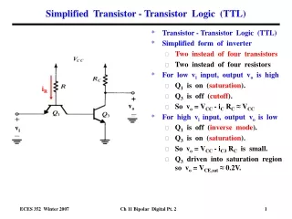
h-Parameters for CE Amp. • hie = the base input impedance • hfe = the base-to-collector current gain • hoe = the output admittance • hre = the reverse voltage feedback ratio
Small signal Amplifier Basic Features Taking Example of Practical C E Amplifier Circuit Input Signal Source
How a small signal amplifier can amplify the weak AC input signal (A practical example taking Common-Emitter Amplifier) If changes in operating currents and voltages are small enough, then IC and VCE waveforms are undistorted replicas of the input signal. A small voltage change at the base causes a large voltage change at the collector. The voltage gain is given by: The minus sign indicates a 1800 phase shift between input and output signals. An 8 mV peak change in vBE gives a 5 mA change in iB and a 0.5 mA change in iC. The 0.5 mA change in iC gives a 1.65 V change in vCE .
Role of Coupling and Bypass Capacitors in BJT Amplifier Coupling Capacitors In a practical amplifier design, C1 and C3 are coupling capacitors . These Capacitors completes two basic task:- 1-They blocks DC signals 2-They pass AC Bypass Capacitors C2 is a bypass capacitor. It provides a low impedance path for ac current from emitter to ground. It effectively removes RE (required for good Q-point stability) from the circuit when ac signals are considered.
So we can conclude Small signal Amplifier Basic Features Taking Example of Practical C E Amplifier Circuit 1-This Give very high Amplification due to high current gain 2- Provide 180 Degree phase change between input and output 3-Use of coupling & bypass capacitor make circuit more useful
Distortion- The change of output wave shape from the input wave shape of an amplifier is known as distortion
D C Equivalent for the BJT Amplifier (Step1) • All capacitors in the original amplifier circuit are replaced by open circuits, disconnecting vI, RI, and R3 from the circuit and leaving RE intact. The the transistor Q will be replaced by its DC model. DC Equivalent Circuit
A C Equivalent for the BJT Amplifier (Step 2) Ro R1IIR2=RB Rin • Coupling capacitor CC and Emitter bypass capacitor CE are replaced by short circuits. • DC voltage supply is replaced with short circuits, which in this case is connected to ground.
A C Equivalent for the BJT Amplifier (continued) All externally connected capacitors are assumed as short circuited elements for ac signal • By combining parallel resistors into equivalent RBand R, the equivalent AC circuit above is constructed. Here, the transistor will be replaced by its equivalent small-signal AC model (to be developed).
1)Determine DC operating point and calculate small signal parameters 2) Draw the AC equivalent circuit of Amp. • DC Voltage sources are shorted to ground • DC Current sources are open circuited • capacitors are short circuits • inductors are open circuits 3) Find the simplified form of network which is a two port network 4) Replace transistor with small signal model 5) Simplify the circuit as much as necessary. Steps to Analyze a Transistor Amplifier 6)Calculate the small signal parameters and gain etc. A C Analysis of CE Amplifier Step 1 Step 2 Step 3 Step 4 Step 5 π-model used