1 / 32

Thin Film Deposition

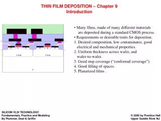
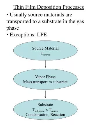
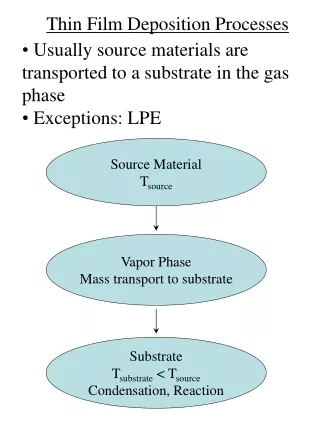
Thin Film Deposition. Types of Thin Films Used in Semiconductor Processing. Thermal Oxides Dielectric Layers Epitaxial Layers Polycrystalline Silicon Metal Films. Uses for Deposited Films. Dielectric Films. Used for insulation and passivation

sparksa
Download Presentation

Thin Film Deposition

An Image/Link below is provided (as is) to download presentation Download Policy: Content on the Website is provided to you AS IS for your information and personal use and may not be sold / licensed / shared on other websites without getting consent from its author. Content is provided to you AS IS for your information and personal use only. Download presentation by click this link. While downloading, if for some reason you are not able to download a presentation, the publisher may have deleted the file from their server. During download, if you can't get a presentation, the file might be deleted by the publisher.

E N D

Presentation Transcript


  1. Thin Film Deposition

  2. Types of Thin Films Used in Semiconductor Processing Thermal Oxides Dielectric Layers Epitaxial Layers Polycrystalline Silicon Metal Films

  3. Uses for Deposited Films

  4. Dielectric Films • Used for insulation and passivation • Typically deposited via atmospheric pressure CVD, low pressure CVD, and plasma-enhanced CVD • Typical films include: • Silicon Dioxide • Silicon Nitride • Low dielectric constant materials • High dielectric constant materials

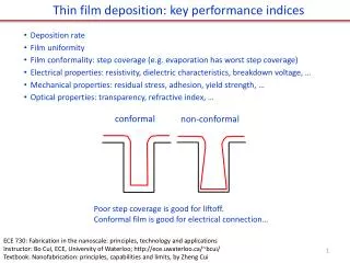
  5. Epitaxy • Related to silicon crystal growth • Single-crystal semiconductor layer is grown on a single-crystal substrate • Homeoepitaxy if grown layer and substrate layer are the same • Heteroepitaxy if the grown layer and substrate layer are different • Done via: • Chemical Vapor Deposition (CVD) • Molecular Beam Epitaxy (MBE)

  6. Lattice Matching Issues in Epitaxy

  7. Critical Layer Thickness for Defect-Free Strained Layer Epitaxy

  8. Why usePolysilicon?

  9. Metal Connections

  10. Deposition Requirements

  11. Deposition Issues

  12. Deposition Issues

  13. Deposition Issues Are Related to Aspect Ratio of Features

  14. Industry Roadmap

  15. Deposition Tools

  16. Atomospheric Pressure Chemical Vapor Deposition (APCVD) Hardware

  17. Improving APCVD Uniformity

  18. Steps in a CVD Process

  19. Silicon Doping with Arsenic and CVD Film Growth process

  20. Silicon APCVD Growth Rates

  21. APCVD Modeling

  22. Alternative Hardware(Low Pressure CVD – LPCVD)

  23. LPCVD vs. APCVD

  24. Plasma Enhanced CVD

  25. High Density Plasma CVD

  26. Physical Vapor Deposition (PVD)

  27. PVD

  28. PVD

  29. DC Sputter Deposition

  30. RF Sputter Deposition

  31. Benefit of an RF Sputter Deposition Tool

  32. Deposition Tools and Conditions for Common Films

More Related