Download
1 / 43
950 likes | 2.17k Views
Thin film deposition: key performance indices. Deposition rate Film uniformity Film conformality : step coverage (e.g. evaporation has worst step coverage) Electrical properties: resistivity, dielectric characteristics, breakdown voltage, …

E N D
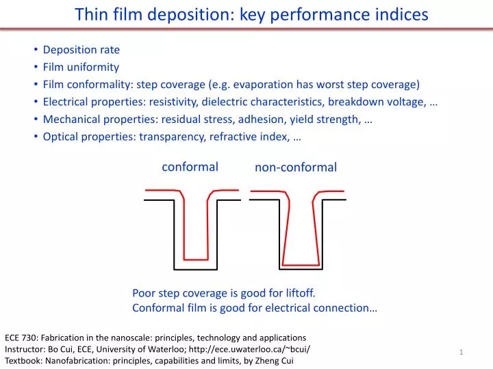
Thin film deposition: key performance indices • Deposition rate • Film uniformity • Film conformality: step coverage (e.g. evaporation has worst step coverage) • Electrical properties: resistivity, dielectric characteristics, breakdown voltage, … • Mechanical properties: residual stress, adhesion, yield strength, … • Optical properties: transparency, refractive index, … conformal non-conformal Poor step coverage is good for liftoff. Conformal film is good for electrical connection… ECE 730: Fabrication in the nanoscale: principles, technology and applications Instructor: Bo Cui, ECE, University of Waterloo; http://ece.uwaterloo.ca/~bcui/ Textbook: Nanofabrication: principles, capabilities and limits, by Zheng Cui
Thin film deposition processes • Physical vapor deposition (PVD) • Evaporation • Sputtering • Chemical vapor deposition (CVD) • Low pressure CVD • Plasma enhanced CVD • Epitaxial deposition • MBE (molecular beam epitaxy) • MOCVD (Metal-Organic CVD)
Equilibrium growth modes (important only for epitaxy) (wetting properties) • Noble metals don’t bond (“wet”) to Si/SiO2 substrate, so tend to have island growth. • Ag always form island (not continuous film); Au is better than Ag. • Adhesion layer Ti or Cr can reduce island formation, but for Ag surface is still very rough. • Here, higher adhesion is because Ti or Cr bond chemically to O in SiO2.
Physical vapor deposition (PVD): evaporation and sputtering • Evaporation: • Material source is heated to sublimation temperature in vacuum either by thermal or e-beam methods. • Material is vapor transported to target in vacuum. • Easier to change evaporation material than sputtering target. • Sputtering: • Material is removed from target by momentum transfer. • Gas molecules are ionized in a glow discharge (plasma), ions strike target and remove mainly neutral atoms. • Sputtered atoms condense on the substrate. • Not in vacuum, gas (Ar) pressure 5-50mTorr.
Assume a particle of diameter s, moving in speed v, wafer Collision cross-section=ps2 Collision volume swept=ps2vdt Collision freq=(n/V)ps2vdt v In more rigorous treatment, 2s source Evaporation: vacuum pressure and mean free path Average mean free path l=vDt = [(n/V)ps2]-1 Assume s = 3Å, T= 300K If l=30 cm, then a pressure <2.6x10⁻⁴Torris required. Typical vacuum <510-6Torr P(Torr)(m) = 7.8x10⁻⁵ 1Torr = 1mmHg = 1/760atm
Arrival ratio Arrival Ratio: ratio of molecular vapor arrival at 1nm/sec deposition rate to molecular impact of residual gas.
Deposition uniformity E.g: for 100mm wafer, if Ro=40cm, tan=5/40, significant shadow effect at wafer edge. This shadowing effect makes liftoff difficult, and modifies feature size.
Thermal evaporation • Materials are evaporated from heated crucible (resistance heating). • Suitable for high vapor pressure metals, e.g. Au, Al,… • Good for organic materials (organic semiconductors…) • Major issues • High contamination level • Can’t work on composite films • Limited choice of materials High contamination: the crucible is heated as well, so may deposit to the substrate. On the contrary, e-beam evaporation heats only the evaporate material from the top.
Electron beam evaporation • Using a focused electron beam to heat and evaporate metals, electron temperature can be as high as 10,000 K. • Suitable for high Tmelt metals like W, Ta, … • Evaporation occurs at a highly localized point on the source surface, so little contamination from the crucible • Composite films can be deposited using dual e-beams with dual targets • Thickness uniformity can be improved by substrate rotation. • Issues: radiation damage; not suitable for organic materials.
Evaporation characteristics of materials For research, typical deposition rate is only 1Å/sec, for film thickness <100nm. For crucible, one can just use graphite for most materials, unless carbon contamination is a major issue. . From “Materials science of thin films” by Ohring, 2002.
Key considerations of evaporation • Deposition rate. • Temperature: some metals requires excessive high temperature. • Contamination control. • Residual stresses: usually of CTE and micro-structures transformation. (CTE: coefficient of thermal expansion) • Evaporation is the most useful thin film deposit techniques for nanofabrication, because: • It is directional (poor step coverage), good for liftoff. • It is directional, good for shadow evaporation. • The film thickness can be monitored precisely using a quartz balance. • Best suitable for elemental materials (metals, silicon, Ge…), not so good for composite (SiO2 → SiOx). Sputtering is suitable for deposition of composite materials. • Film quality is generally not as good as sputtered film (that involves energetic bombardment of ions to the as-deposited film, which makes the film denser).
GLAD (glancing angle deposition): self assembly of film Angle >80o, with substrate rotation. Self assembly mainly due to shadowing effect that magnifies the otherwise grain structures. Invented by Michael Brett from University of Alberta http://www.ece.ualberta.ca/~glad/lab.html
Sputtering (overview) Vacuum chamber Substrate Target • Sputter is carried out in a self-sustained glow discharge (plasma). • The ionized atoms bombard the target and cause the transport of sputtered atoms onto the substrate. • Advantages: • Able to deposit a wide variety of metals, insulators and composites. • Replication of target composition in the deposited films. • Capable of in-situ cleaning prior to film deposition by reversing the potential on the electrodes . • Better film quality and step coverage than evaporation, preferred deposition technique for micro-fabrication (semiconductor industry…). • Disadvantages: • Substrate damage due to bombardment Electrode Electrode Flow rate controller RF power generator
Sputtering process • Heavy inert gas is the major carrier, e.g. Ar. • Reactive chemical species (e.g. O2 to deposit oxide) may be introduced – reactive sputtering • Sputtering process can be run in DC or RF mode (insulator must be run in RF mode) • Major process parameters: • Operation pressure (~10-100mTorr) • Power (few 100W) • Substrate bias (in addition to self-bias) • Substrate temperature (20-500oC) • Dielectric materials can also be deposited, but are usually formed by sputtering metals in O2 , N2, CH4 gases, forming AlN, Al2O3, TiN, TiC… • A wide range of industrial products use sputtering: CD,LCD, computer disks, hard coatings for tools, metals on plastics.
Sputter yield (higher yield → higher deposition rate) • Sputter yield: the number of sputtered atoms per impinging ion. • Energy of each incoming ion is 500-1000eV.Energy of sputtered atoms is 3-I0eV. Sputter yield is 1-3. • Thus, 95% ofincoming energy goes to target heating & secondary electron. • High rate sputter processes need efficient cooling techniques to avoid target damage from overheating. • Ion energy↑, sputteringyield↑ Sputter yield vs. ion energy for Ar ions
DC Sputtering • Deposition parameters: • Process pressure: compromise between the number of Ar ions and the scattering of Ar ions with neutral Ar atoms • Sputter voltage: maximum yield, typical -2 to -5 kV, for high deposition rate. • Substrate bias: control ion bombardment characteristics. • Substrate temperature: modify deposited film properties. • For conducting materials only.
RF Sputter • Good for insulating materials because, positive charge builds up on the cathode (target) in DC sputtering systems. Alternating potential can avoid charge buildup • When frequencies less than about 50kHz, electrons and ions in plasma are mobile • DC sputtering of both surfaces • When frequencies above about 50kHz, ions (heavy) can no longer follow the switching • Electrons can neutralize positive charge build up. • Capable of running in lower pressure (1-15 mTorr) 13.56MHz RF source, same as RIE or PECVD
Chemical vapor deposition (CVD) • Form thin films on the surface of a substrate by thermal decomposition and/or reaction of gaseous compounds • Usually performed at high temperature • Can be performed at various pressure and with assistance of plasma (PECVD) • CVD film growth steps • Source production of appropriate gas • Transport of gas to surface • Adsorption of gas on substrate • Reactions on substrate • Transport of by-products away from substrate
Types of CVD reactions • Thermal decomposition • AB(g) ---> A(s) + B(g) • ex: Si deposition from Silane at 650oC: SiH4(g) → Si(s) + 2H2(g) • Reduction (using H2) • AX(g) + H2(g) <===> A(s) + HX(g) • W deposition at 300oC: WF6(g) + 3H2(g) <===> W(s) + 6HF(g) • Oxidation (using O2) • AX(g) + O2(g) ---> AO(s) + [O]X(g) • SiO2 deposition from silane and oxygen at 450oC (lower temp than thermal oxidation): SiH4(g) + O2(g) ---> SiO2(s) + 2H2(g) • Compound formation (using NH3 or H2O) • AX(g) +NH3(g) --> AN(s)+HX(g) or AX(g)+H2O(g)-->AO(s)+HX(g) • Deposit wear resistant film (BN) at 1100oC: BF3(g) + NH3(g) ---> BN(s) + 3HF(g)
CVD sources and substrates • Types of sources • Gasses (easiest) • Volatile liquids • Sublimable solids • Combination • Source materials should be • Stable at room temperature • Sufficiently volatile • High enough partial pressure to get good growth rates • Reaction temperature < melting point of substrate • Produce desired element on substrate with easily removable by-products • Low toxicity • Substrates • Need to consider adsorption and surface reactions • For example, WF6 deposits on Si but not on SiO2
Mass transport in gas • Two flow Regimes • Molecular flow (diffusion in gas) • Viscous flow (laminar flow and turbulent flow) • Laminar flow is desired. • Reactants diffuse through stagnant layer to surface Mass Transport depends on D is diffusivity dc/dx is the concentration gradient across the boundary layer that separates the bulk flow (source) and the substrate surface (sink). In a LPCVD reactor (~1Torr), the diffusivity (D) of the gas species is increased by a factor of 1000 over that at atmospheric pressure, resulting in one order of magnitude increase in the transport of reactants to the substrates.
Mass transfer control Growth rate Surface reaction control Substrate temperature, 1/T Growth limiting step • At lower temperature, surface reaction is the control mechanism: temp↑, growth rate ↑ • At higher temperature, bulk transportation/ diffusion is the control mechanism: flow rate ↑, growth rate ↑ Pressure dependence of CVD deposition rate LPCVD: low pressure CVD APCVD: atmospheric pressure CVD high gas pressure, high deposition rate, limited by mass transport.
CVD process • Advantages: • High growth rates possible • Can deposit materials which are hard to evaporate • Good reproducibility • Can grow epitaxial films (in this case also termed as “vapor phase epitaxy (VPE)”. For instance, MOCVD is also called OMVPE.) • Generally better film quality than PVD films. • Disadvantages: • High process temperatures • Complex processes • Toxic and corrosive gasses • Film may not be pure (hydrogen incorporation…).
Types of CVD • APCVD (Atmospheric Pressure CVD) (not very popular for nanofabrication), mass transport limited growth rate, leading to non-uniform film thickness. • LPCVD (Low Pressure CVD) • Low deposition rate limited by surface reaction, so uniform film thickness (many wafers stacked vertically facing each other; in APCVD, wafers have to be laid horizontally side by side. • Gas pressures around 1-1000mTorr (lower P => higher diffusivity of gas to substrate) • Better film uniformity & step coverage and fewer defects • Process temperature 500°C • PECVD (Plasma Enhanced CVD) • Plasma helps to break up gas molecules: high reactivity, able to process at lower temperature and lower pressure (good for electronics on plastics). • Pressure higher than in sputter deposition: more collision in gas phase, less ion bombardment on substrate • Can run in RF plasma mode: avoid charge buildup for insulators • Film quality is poorer than LPCVD. • Process temperature around 100 - 400°C. • MOCVD (Metal-organic CVD, also called OMVPE - organo metallic VPE), epitaxial growth for many optoelectronic devices with III-V compounds for solar cells, lasers, LEDs, photo-cathodes and quantum wells.
CVD reactors PECVD LPCVD plasma Reaction at high temperature Reaction rate (determined by temperature) limited deposition rate. Reaction at low temperature, assisted by plasma
PECVD process parameter • Substrate temperature • Control by external heater, very little heating from PECVD process • Gas flow • Higher flow rates can increase deposition rate and uniformity • Pressure • Changes the energy of ions reaching electrodes • Can change deposition rate • Increases pressure may lead to chemical reactions in the gas • Effects also depend on gas concentration • Power • Affects the number of electrons available for activation and the energy of those electrons • Increased power may lead to chemical reactions in gas • Increased power increases deposition rate • Frequency (for PECVD) • Changes plasma characteristics • Changes ion bombardment characteristics
Polycrystalline silicon and silicon dioxide deposition Si • Application: gate of MOSFET, surface micromachining • Usually deposited in a LPCVD chamber at 25-150Pa, 600-650oC, 10-20nm/min. • In situ doping can be performed: usually perform thermal diffusion right after poly-silicon deposition. SiO2 • Silane based • TEOS (LPCVD 650-700°C) (PECVD 350°C) • Silane based PECVD
Comparison of varied silicon dioxide Lower HF etch rate means better film quality (denser film)
Silicon nitride deposition • Application: • Masks to prevent oxidation for LOCOS process • Final passivation barrier for moisture and sodium contamination • Etch stop for Cu damascene process • Popular membrane material by Si backside through-wafer wet etch. • PECVD • LPCVD LPCVD conformal Si3N4films
Atomic layer deposition (ALD, break CVD into two steps) • Similar in chemistry to chemical vapor deposition (CVD), except that the ALD reaction breaks the CVD reaction into two half-reactions, keeping the precursor materials separate during the reaction. • The precursor gas is introduced into the process chamber and produces a monolayer of gas on the wafer surface. A second precursor of gas is then introduced into the chamber reacting with the first precursor to produce a monolayer of film on the wafer surface. • Film growth is self-limited (monolayer adsorption/reaction each half-cycle), hence atomic layer thickness control of film grown can be obtained. • That is, one layer per cycle; thus the resulting film thickness may be precisely controlled by the number of deposition cycles. • Two fundamental mechanisms: • Chemi-sorption saturation process • Sequential surface chemical reaction process • Introduced in 1974 by Dr. TuomoSuntola and co-workers in Finland to improve the quality of ZnS films used in electroluminescent displays. • Recently, it turned out that ALD also produces outstanding dielectric layers and attracts semiconductor industries for making High-K dielectric materials.
ALD cycle for Al2O3 deposition 1. Introduce TMA. (tri-methyl aluminum) In air, H2O vapor absorb on Si to form Si-O-H. 2. TMA reacts with hydroxyl groups to produce methane.
ALD cycle for Al2O3 deposition 3. Reaction product methane is pumped away, leaving an OH-passivation layer on surface. 2. After three cycles. One TMA and one H2O vapor pulse form one cycle. Here ~1A/cycle, each cycle including pulsing and pumping takes few seconds. Two steps each cycle
Closed system chambers (most common) for ALD • The reaction chamber walls are designed to effect the transport of the precursors.
Advantages and disadvantages ALD: slowest, best step coverage • Advantages • Stoichiometric films with large area uniformity and 3D conformality. • Precise thickness control. • Low temperature deposition possible. • Gentle deposition process for sensitive substrates. • Disadvantages • Deposition rate slower than CVD. • Number of different material that can be deposited is fair compared to MBE.
Pulsed laser deposition (PLD) Co-deposition
Plume generated by laser ablation with different tiny or micro-particles Pulse of fs to ns with peak power high enough (hundreds of MW/cm2) to melt → boil → vaporize → ablate the target surface material, to atoms, ions, electrons, and clusters. Laser Beam Target Plume (Plasma) (b) (c) (d) (a) • Figure 5.1. Schematic laser-material interaction. (a) Absorption and heating; (b) Melting and flowing; (c) Vaporization; (d) Plasma formation in front of the target. Under certain conditions the plasma can detach from the target and propagate toward the laser beam. Substrate • PLD Characteristics: • Reproduce the composition of the target • Fabricate multi-component multilayer structures • Fast response and well controlled deposition rate • Environmentally benign technique
Transient plume development with and without reaction gas 10-6Torr vacuum 100 mTorr O2 D. Geohegan, Appl. Phys. Lett. 60, 2732 (1992)
Pulsed laser deposition (PLD) system(pulsed excimer laser and chamber) View Windows Laser Chamber
Working Electrode (WE) Counter Electrode (CE) “Oxidation" Cu(0) –> Cu2+ + 2e- Nano-film by electro-deposition (electroplating) I V cathode anode CuSO4 dissolved in water If using an inert Pt electrode: 2 H2O –> O2 + 4H+ + 4e- “Reduction" Cu2+ + 2e- –> Cu(0)