Download

1 / 32
320 likes | 452 Views
Recent Topics on Programmable Logic Array. Ulkuhan Ekinciel Asada Lab. M1 Electronics Eng. Dept. University of Tokyo. OUTLINE OF PAPER. Introduction Brief Review of PLA Concepts Control Logic Implementation and Timing Closure with PLA Crosstalk-Immune Design in PLA Network Summary.

E N D
Recent Topics on Programmable Logic Array Ulkuhan Ekinciel Asada Lab. M1 Electronics Eng. Dept. University of Tokyo
OUTLINE OF PAPER • Introduction • Brief Review of PLA Concepts • Control Logic Implementation and Timing Closure with PLA • Crosstalk-Immune Design in PLA Network • Summary
Introduction 1 • PLAs provide a regular structure. • They require a small number of separate cell designs. • They allow for ease of testing while offering simple, rapid expandability. • The regular array structure makes the PLA’s timing predictable. • PLAs can implement almost any Boolean function.
However with the decreasing minimum feature size of VLSI fabrication, some problems are becoming increasingly common Cross-talk Self-heat Electromigration Statistical Process Variations And etc… Introduction 2
Introduction 3 • The increasing importance of these electrical effects requires that designers consider the interaction between logical and physical design at the same time.
OUTLINE OF PAPER • Introduction • Brief Review of PLA Concepts • Control Logic Implementation and Timing Closure with PLA • Crosstalk-Immune Design in PLA Network • Summary
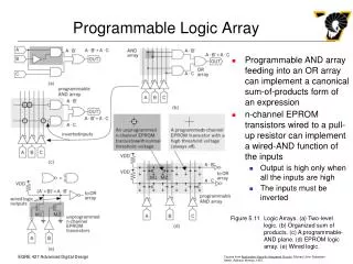
Brief Review of PLA Concepts • A PLA maps a set of Boolean functions in canonical, two-level sum-of-product form into a geometrical structure. • A typical PLA consists of two major sections or planes. One is called the ‘AND’ plane and the other is called ‘OR’ plane. • The AND plane is responsible for generating the product term while the OR plane sums the required terms.
Design Styles 1 • Static NMOS and Pseudo-NMOS PLA • INV-NOR-NOR-INV • High Static Power dissipation • Small area • Useful if high speed is not required • NAND-NAND • NAND-NAND approach is not recommended • Decreasing performance at increasing number of inputs (because of series connection of NMOS transistors) • High static power dissipation
Design Styles 2 • Static CMOS PLA • No static power dissipation • Area increase becomes unacceptable for large PLA’s • Working Fast • Dynamic CMOS PLA • Less size than static CMOS • Fast • 2-phase clocking
Design Styles 3 Pseudo-Static PLA Dynamic PLA
Noise in PLA • In dynamic PLAs noise problems are on switched supply lines • Discharging current is generating in the power supply bus • To reduce noise: Locally groundingthe PLA use of the metal lines for power supply whenever possible (reduced impedance)
PLA Generation • PLA Generation is a process by which a set of input signals combines, through a logical sum of products, to form a set of output signals.
OUTLINE OF PAPER • Introduction • Brief Review of PLA Concepts • Control Logic Implementation and Timing Closure with PLA • Crosstalk-Immune Design in PLA Network • Summary
Control Logic Implementation and Timing Closure with PLA • Potential timing closure problems due to random control logic can be avoided through the use of structured arrays with predictable electrical characteristics.Because array structures are an ideal place to use dynamic circuits. • Timing can be very structured, • Path length is very well known, • And physical dimensions are fixed
Timing closure for large microprocessor design is becoming more and more difficult as Chip complexity increases Cross-chip wire delays become more significant Dynamic Circuits become more prevalent Cycle times shorten The ‘Timing Closure by Design’ methodology has the goals of Achieving the highest possible processor frequency Reducing the design time to achieve that desired frequency The main themes of this methodology are: Early timing planning with an eye towards the physical implementation Using components and design techniques with predictable timing characteristics Timing Closure by Design S. Posluszny et al. DAC 2000
Characteristic of ‘Timing Closure by Design’ • Logical partitioned on timing boundaries • Predictable Control Structures (PLAs) • Static Interfaces for Dynamic Circuits • Low skew clock distribution • Deterministic Method of macro placement • Simplified timing analysis • Refinement method of chip integration with early timing analysis
Control Template • No heuristic logic synthesis or auto placement is required with PLAs or comparators. • The PLAs have exclusive latch drivers, which are placed adjacent to the PLAs, minimizing input wire delays and consequently input skews. • For increasing functionality without significantly adding delay uncertainty, due to the high performance of the PLAs, a single level static or dynamic gate can be connected to the PLA outputs.
Design Methodology for a 1.0 GHz Microprocessor S.Posluszny et. al. Int. Conf. On Computer Design 1988 • PLA’s macros use dynamic circuits to meet their timing requirements. Dynamic PLAs provide: • High frequency operation • Quick logic implementation • Predictable area and delay • Early recognition of excess logic for one cycle. • The stated reasons to implement PLAs to control logic are high speed and the ability to be quickly implemented and this modifies the design.
Processor Organization • In this design as much control logic as possible is combined within the data-path macros. The rest of the control is partitioned so that it does not need to merge with the datapath other than at the end of the cycle. This in turn allows the control logic to use of ROMs and PLAs for control implementation.
Chip Micrograph • The figure shows a chip micrograph with the major macros. The PLA structures used in the CU (Control Unit) part of this chip. • All the chip level macros are hand placed to control and predictable wire delays and noise across the chip.
Comparison of Static Standard Cell and Dynamic Arrays • In the table, there is a comparison of static random-logic macros (RLMs) using standard cells and dynamic structured arrays (ROMs and PLAs)
OUTLINE OF PAPER • Introduction • Brief Review of PLA Concepts • Control Logic Implementation and Timing Closure with PLA • Crosstalk-Immune Design in PLA Network • Summary
Crosstalk-Immune Design in PLA S.P. Khatri Int. Conf. CAD 2000 Network • Occurrence of Cross-talk • Cross-talk typically occurs between adjacent wires on the same metal layer, when the cross-coupling capacitance between these wires is large enough to affect each other’s electrical characteristics. • With the decreasing VLSI size, the height of the wires are increasing, in order to keep their sheet resistivity from increasing quadratically. This is in turn increases the cross-coupling capacitance between a wire and its neighbors as a fabrication of its total capacitance, resulting in cross-talk problems.
Effects of Cross-talk • In particular cross-talk can cause a significant delay variation in a wire depending on the state of neighboring wires. • Also, it can cause the logic value of a wire to be incorrectly interpreted depending on the state of neighboring aggressor wires, resulting in a loss of a signal integrity.
Dense Wiring Fabric (DWF) • Solution • Dense Wiring Fabric (DWF) The cross-talk elimination can be done by imposing a fixed pattern of wires on the IC die, on all metal layers. This ensures that adjacent signal wires are always capacitively shielded form each other.
Approach • In this scheme, the circuit is implemented as a network of PLAs. • The routing region between PLAs is organized using the DWF, giving rise to highly predictable, crosstalk-immune routes. • Intersecting VDD or GND wires on adjacent layers are connected by vias. This gives rise to a highly efficient power and ground distribution network throughout the die.When PLAs are placed, local breaks occur in the power and ground gridding structure of Metal 1 and Metal 2.
PLAs in DSM VLSI Design • The pre-charged NOR-NOR PLA is used in this design. By using NOR-NOR PLA as the layout building block, no extra area penalty is incurred, either in the horizontal and vertical direction. • The structure of PLA is crosstalk immune.
Layout Plan • The layout of PLA core is implemented by using two metal layers. • The width of the PLA core is 4.n+2.m tracks, since the each input requires 4 vertical tracks, and each output requires 2.
Arrangement of Conductors • In this methodology the arrangement of conductors in PLA core is like as shown in the next figure.
Advantages of Presented Method • High Speed • Low area overhead • High reliability • Rapid design • Power and ground routing is done implicitly, and not in a separate step • Variations in delay of a signal wire due to switching activity on its neighboring signal wires less than conventional layout techniques • Smaller and uniform inductances for all wires on the chip • There is no intervening technology mapping step. This helps ensure that benefits due to synthesis optimizations are not lost in the implementation step
OUTLINE OF PAPER • Introduction • Brief Review of PLA Concepts • Control Logic Implementation and Timing Closure with PLA • Crosstalk-Immune Design in PLA Network • Summary
Summary • General PLA concept was briefly reviewed • Some samples from recent papers on PLA were introduced • Usage of PLA in control logic unit • In Gigahertz technology timing closure problem overcoming with PLA structures • Crosstalk-immune design in PLA network