Download

1 / 16
160 likes | 430 Views
Ovonic Unified Memory. What is ovonic unified memory?. Ovonic unified memory(also known as PCM , PRAM , PCRAM , Phase-change memory and Chalcogenide RAM C-RAM ) is a type of non volatile memory which uses a unique thin-film phase change material to store information .

E N D
What is ovonic unified memory? • Ovonic unified memory(also known as PCM, PRAM, PCRAM, Phase-change memory and Chalcogenide RAM C-RAM) is a type of non volatile memory which uses a unique thin-film phase change material to store information . • PRAM uses the unique behavior of Chalcogenide glass, which can be "switched" between two states, crystalline and amorphous, with the application of heat . • OUM is based on the information storage technology that allows rewriting of CD's and DVD's.
While CD and DVD drives read and write ovonic material with lasers, OUM uses electric current to change the phase of memory cells.
What is a non volatile memory? • Non-volatile memory is the general name used to describe any type of memory which does not lose its information when power is turned off. • NVRAM(non volatile random access memory) is a subgroup of the more general class of non-volatile memory types, the difference being that NVRAM devices offer random access, as opposed to sequential access like hard disks. • The best-known form of NVRAM memory today is flash memory used in camera’s,scan devices and flash drives.
Why chalcogenide glasses ? • The crystalline and amorphous states of chalcogenide glass have dramatically different electrical resistivity values, and this forms the basis by which data are stored. • The amorphic, high resistance state is used to represent a binary 0, and the crystalline, low resistance state represents a binary 1 . • Chalcogenide is the same material utilized in re-writable optical media (such as CD-RW and DVD-RW). In those instances, the material's optical properties are manipulated, rather than its electrical resistivity, as chalcogenide's refractive index also changes with the state of the material.
How chalcogenide glass switches states? It is heated to a high temperature (over 600°C), at which point the chalcogenide becomes a liquid. Once cooled, it is frozen into an amorphic glass-like state and its electrical resistance is high. By heating the chalcogenide to a temperature above its crystallization point, but below the melting point, it will transform into a crystalline state with a much lower resistance. This phase transition process can be completed in as quickly as five nanoseconds
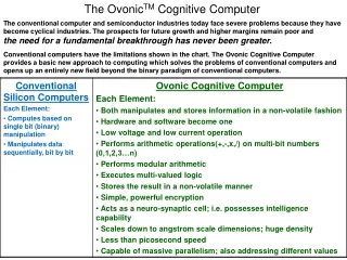
Structure of FLASH memory • Flash memory works by modulating charge (electron) stored within the gate of a MOS transistor . • The gate is constructed with a special "stack" designed to trap charges . • Changing the bit's state requires removing the accumulated charge, which demands a relatively large voltage to "suck" the electrons off the floating gate. This burst of voltage is provided by a charge pump which takes some time to build up power. • write times for common Flash devices are on the order of one ms (for a block of data), about 100 000 times the typical 10 ns read time (for a byte).
PRAM can offer much higher performance in applications where writing quickly is important, both because the memory element can be switched more quickly, and also because single bits may be changed to either 1 or 0 without needing to first erase an entire block of cells which makes it effectively 30-times faster than flash memory A PRAM device may endure around 100 million write cycles. Flash memory erases the entire data block. With Flash, each burst of voltage across the cell causes degradation, so most flash devices are only rated for something on the order of 10 000 to 100 000 writes per sector, PRAM vs FLASH memory
PRAM exhibits higher resistance to radiation. PRAM requires 20 percent fewer process steps than those for the manufacturing of NOR flash, making it cheaper to produce Flash devices trap electrons to store information, they are susceptible to data corruption from radiation, making them unsuitable for many space and military applications . More processing steps to fabricate a flash memory
Where can PRAM’s be useful? • PRAM is a promising technology in the military and aerospace industries where radiation effects make the use of standard non-volatile memories such as Flash impractical . • A write cycle endurance of 10^8, which will allow it to be a contender for replacing PROM’sand EEPROMs in space systems. • Other potential PRAM applications include much faster and capacious USB thumb drives and solid-state disk drives . • Hybrid disk drives and the motherboard with flash cache, could also have larger and significantly faster cache memory leading to better performance.
PRAM is expected to be especially popular in the future designs of multi-function handsets and for other mobile applications .
Fundamental tradeoff: unintentional vs. intentional phase-change • PRAM lifetime is limited by mechanisms such as degradation due to GST thermal expansion during programming, metal (and other material) migration, and other mechanisms still unknown. • The contents of a PRAM are lost because of the high temperatures needed to solder the device to a board. The manufacturer using PRAM parts must provide a mechanism to program the PRAM "in-system" after it has been soldered in place.
Reference www.BAEsystems.com www.samsung.com www.techworld.com