Download
1 / 23
230 likes | 234 Views
New Transformative Possibilities for Ovonic Devices. Stanford R. Ovshinsky Ovshinsky Innovation, LLC EPCOS 2010 Milan, Italy. Introduction.

E N D
New Transformative Possibilities for Ovonic Devices Stanford R. Ovshinsky Ovshinsky Innovation, LLC EPCOS 2010 Milan, Italy
Introduction I know of no better place to give this kind of talk than Italy where I have had some of my happiest memories of working together with Giulio Casagrande, Paolo Cappelletti, Roberto Bez, Fabio Pellizzer and their wonderful colleagues and collaborators. I felt the same kind of warmth that I had in Japan with the splendid group that did such a great job building the optical phase change memory industry. Many are in this audience. My paper is more complex than I usually present so I will seek to summarize its significance to you here, but please read the paper which is in your package. OVSHINSKY INNOVATION
Introduction The Ovonic Phase Change Memory is critical in the quest to meet the increasing commercial needs for new information systems. The important paper of DerChang Kau et al. [1], describing a stackable cross point phase change memory, resulting in a three dimensional device which includes the Ovonic Threshold Switch, as an access device, demonstrates the possibility for significant expansion of our field through the use of OTS. [1] D. Kau, et al. “A stackable cross point phase change memory,” Electron Devices Meeting (IEDM), 2009 IEEE International, DOI: 10.1109/IEDM.2009.5424263 (2009) OVSHINSKY INNOVATION LLC
A Stackable Cross Point Phase Change Memory In a recent paper, Intel introduced the Ovonic Threshold Switch with phase change memory [1], showing the three dimensionality that can be achieved with those devices, as shown here. (from Intel) OVSHINSKY INNOVATION LLC
Logic Devices A logic device is like a black box with 2 inputs and 1 output which is usually implemented using transistor gates. A truth table describes this behavior of the logic gates in terms of binary inputs and outputs. In the next slide I give an example of IMP logic where: If you input 0, 0 it outputs 1 If you input 0, 1 it outputs 1 etc. OVSHINSKY INNOVATION
IMP Logic Many of you in the audience have heard me discuss through the years the fact that we can make with our Ovonic devices and mechanisms circuits that not only do non volatile memory but also do logic. Just recently there has been an announcement by Hewlett Packard in which they feature devices known as memristors capable of doing both logic and memory [2]. Their claim is that they can implement what is called IMP logic operation (‘logic by implication’ or p implies q type logic). The truth table for that kind of logic is shown here. OVSHINSKY INNOVATION LLC
What I want to prove in this presentation is that the properties of both the 2-terminal OTS and 2-terminal OMS devices can be described in terms of the devices being memristors. As such they can be used as memory devices and that is what our Ovonic memory is. With an additional third electrode they become logic devices and I will show that IMP logic can be performed by a single 3-terminal OTS or a single 3- terminal OMS device (instead of 3 memristors as in the Hewlett Packard [2]). OVSHINSKY INNOVATION LLC
What I want to show here is that: 1/ The 2-terminal Ovonic Threshold Switch behaves like a memristor for voltages close to the threshold voltage. 2/ The cognitive mode of operation of the 2-terminal Ovonic Memory Switch (the Ovonic cognitive memory device) is a memristor device. 3/ The 3-terminal OMS device executes IMP logic (p implies q) in a single device – the same logic that HP claims 3 of their memristor devices are required to execute. 4/ The 3-terminal OTS device in ‘latching’ mode can be used not only as a replacement for the access transistor to the OMS bit (as shown in a recent important paper by Intel), but to perform the same IMP logic, as well as other logic functions. 5/ The difference, compared to the 3-terminal OMS-type logic, is that the 3-terminal OTS device does not store the result in a non-volatile fashion. On the other hand this logic can be extremely fast. (Faster than the OMS logic, because it does not involve a phase change.) In fact, it is so fast, it has never been measured. OVSHINSKY INNOVATION LLC
First, what is a memristor? The Memristor is also called the fourth basic circuit element (along with resistor, capacitor and inductance). Its existence was first hypothesized by Chua in 1971 [3]. In this paper the 2-terminal OTS device is referenced as a possible example of a memristor and my 1968 paper was cited. In a circuit the memristor implements the relationship between magnetic flux ‘f’ and electric charge ‘q’: M(q) = df(q)/dq M(q) has the dimension of resistance and is called ‘memristance’ – or resistance with memory. The reason for that is that, being a function of electric charge, ITS VALUE AT ANY TIME IS DETERMINED BY THE CURRENT THROUGH THE DEVICE FOR ALL PREVIOUS TIMES. IN OTHER WORDS IT IS A RESISTANCE WITH MEMORY – IT STORES THE INFORMATION ABOUT ITS PAST IN ITS VALUE. It should also be noted that if f(q) is a linear function of q, M(q)=R is a constant and the memristor becomes a ‘normal’ resistor. THEREFORE, THE MEMRISTOR SHOULD BE DEFINED AS A NON-LINEAR RESISTOR WITH MEMORY. OVSHINSKY INNOVATION LLC
3-Terminal OTS/OMS Device Top terminal 3rd terminal Thermal Oxide Bottom terminal Si Wafer We will discuss a version of the OTS device with three terminals, as shown here. We will show that a 3-terminal OTS device can both be used as a replacement for a transistor and as an access device to an OMS bit, and perform the inverse logical IMP operation. OVSHINSKY INNOVATION LLC
I(V) Curves for a 3-terminal OTS Device Here I will show that a 3-terminal Ovonic Threshold Switch can replace conventional transistors of all types with very definite advantages. One can see from the I(V) curves that we can modulate both the threshold voltage and the holding current of the device by applying bias on the third terminal. OVSHINSKY INNOVATION LLC
3-Terminal OTS Latching Mode Pulse on 3-terminal Pulse top to bottom OFF Latched “ON” This is an example of a 3-terminal OTS device operation in the so-called ‘latching’ mode. You can see that a 3-terminal threshold switch can be turned on by applying a short pulse on the intermediate terminal which latches the OTS in the on-state. With the OTS in the on-state the memory device can be probed or programmed. Because of that latching property, the 3-terminal threshold switch can be used as a volatile memory bit. Essentially the latching allows the OTS to be ‘on’ without any current through the third terminal, which also saves energy. OVSHINSKY INNOVATION LLC
Truth Table for a 3-Terminal OTS Device Showing Inverse IMP Logic Operation INV(q ‘) pIMPq Because the voltage on the OTS can be switched from high to low (from sub-threshold to the holding voltage), the 3-terminal OTS can show the same IMP logic operation as the memory only essentially it is a volatile memory. Namely, the voltage top to bottom terminal can be high (1) or low (0) and the voltage on the 3rd terminal can be high (1) or low (0). Then, the output voltage top to bottom will be according to the truth table shown here. OVSHINSKY INNOVATION LLC
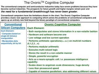
OMS Device – Cognitive and Direct Over-Write Mode Synaptic Cognitive Regime Energy Accumulation Amorphous Pre-threshold Regime Direct Overwrite Reversible Crystalline Multi State Regime S d S d All thin film nanocircuits based upon the new Physics and unique multifunctionality NUMBER OF CONSTANT AMPLITUDE PULSES (Each pulse induces crystallinity) VARIABLE AMPLITUDE PULSES (Each pulse induces amorphicity) Much more uniqueness is available to the Ovonic Unified Memory/ Cognitive Device. As you can see above, there are two regimes of operation of the OUM device – the one on the right is the direct overwrite regime used for non-volatile and multi-state memory. The one on the left is what we call ‘the pre-threshold or cognitive regime’ as well as being binary off and on.’ OVSHINSKY INNOVATION LLC
All this is in a scalable nano-structure device and with three or more terminals it becomes a logic device. In this regime we have shown that the device can be used to perform modular arithmetic and factoring [11]. Based on that functionality we have shown that new types of logic, non binary storage and processing, fast factoring, encryption and other functionality can be developed [12]. All this in a scalable nano structured device. OVSHINSKY INNOVATION
OMS in Cognitive Mode Memristance M(q)=df/dq vs. number of pulses for OMS in cognitive regime If based on the previous slide we plot the memristance of the Ovonic Cognitive Device vs. the number of applied pulses, we get this figure which shows that the Ovonic Cognitive Device acts as a memristor because the resistance of the device in the cognitive regime is a non-linear function of the total charge. The non cognitive or direct over-write mode allows the resetting of the logical zero or ‘false’ state of the device, therefore the entire device acts as a synaptic neuronal system. The device remembers the number of pulses that have been sent to it. The way this information is stored is completely secure since the pre-threshold state cannot be forensically recognized. It is absolutely not-attackable, solving the problem of security. OVSHINSKY INNOVATION LLC
Cognitive Functionality There are a great number of patents in my name as well as my collaborator, Boil Pashmakov, related to 3-terminal OTS and OMS devices. Please, see the references for the patent numbers on Slide 19 [10]. What is shown in these patents is that: Ovonic devices can be used singly and together in circuits to provide a huge range of capabilities • Can adapt some algorithms of quantum devices – ideal for factoring • Addition, subtraction, division, multiplication • Huge parallelism • Weighted interconnections using multi-state phase change storage devices • Search engine • Not just matching, but intelligent searches • Learns as you search • Associative capabilities Ovonic Single and Multiple are unique in that in one device they have both synaptic and neuronal properties Output fires when the threshold is reached by summing the synaptic inputs The Ovonic Threshold switch does this instantly, continuously and reversibly The Ovonic Cognitive Device does this through accumulation of input over time OVSHINSKY INNOVATION LLC / OVONYX
IMP Logic Using 3 Memristors More recently [2] Hewlett Packard came up with a claim for a memristor device that can be used as a non-volatile memory and as a logic device to perform logic by IMP (‘material implication’). They show in this figure, which was taken from their paper [2], that using 3 of their devices they can perform the logical IMP operation (compared to a single OMS device). OVSHINSKY INNOVATION LLC
Truth Table for a 3-terminal OMS Device Showing IMP Logic Operation [4] S. R. Ovshinsky and B. Pashmakov: “Multi-terminal device having logic functional,” U.S. Patent 7,186,998 B2, March 6, 2007 (q ‘) pIMPq We have a patent for a 3-terminal OMS device [4], which incorporates the truth table here and can perform the same logic function as a single device. In this truth table, we have assigned logical ‘0’’ to the ‘reset’ (amorphous or high resistance) state and logical ‘1’ to the ‘set’ (crystalline or low resistance) state. We also input the logical variable ‘p’ in the top-to-bottom contact and the logical variable ‘q’ in the 3t-to-top contact. The result of the logical operation (q’) is read as the output 3t-to-top. OVSHINSKY INNOVATION LLC
Thus, we have shown that a 3-terminal OMS or OTS device can execute the logical operation “material implication” or IMP which combined with the logical false (or device reset), constitutes a computationally complete logic basis which means that all Booleanlogic operations can be done using a single three terminal OMS device [2]. To see the synaptic neuro-physiological analogue of this device, please see my papers in the reference section and [5-7]. OVSHINSKY INNOVATION
Conclusion I have been writing and describing at the EPCOS meetings through the years that the Ovonic Phase Change Memory and Ovonic Threshold Switch and 3-terminal threshold switch are able to accomplish extremely fast switching and that the current density of the solid state plasma of the threshold switch is fifty times higher than conventional transistors. An incredible number that I have indicated and likened to a room temperature dynamic superconductor [8]. This has been briefly discussed here but I’m looking forward to our full discussion at the next meeting. OVSHINSKY INNOVATION LLC
Conclusion • In ending, I have described the unique electronic and phase change mechanisms where the Ovonic Memory has a threshold excitation action and wherein we can integrate in a single synaptic nano-device unique multifunctional circuits. • What I am proposing in this paper is that there is much more richness and depth to the field of Ovonic threshold and memory devices. For example, we have a unified memory and 3-terminal threshold and memory action in which their mechanisms permit the performance of logic and storage of data in the same device, as well as modular arithmetic and factoring which can save much real estate and cost opening a new important chapter in computer cognitive intelligence. Our field and its market can literally be transformed if we use the full inherent proven potential in the Ovonic memory and Ovonic threshold devices. OVSHINSKY INNOVATION LLC
References • D. Kau, S. Tang, I.V. Karpov, R. Dodge, B. Klehn, J.A. Kalb, J. Strand, A. Diaz, N. Leung, J. Wu, S. Lee, T. Langtry, K. Chang, C. Papagianni, J. Lee, J. Hirst, S. Erra, E. Flores, N. Righos, H. Castro and G. Spadini: “A stackable cross point phase change memory,” Electron Devices Meeting (IEDM), 2009 IEEE International, DOI: 10.1109/IEDM.2009.5424263 (2009). • J. Borghetti, G.S. Snider, P.J. Kuekes, J. J. Yang, D. R. Stewart and R.S. Williams: “’Memristive’ switches enable ‘stateful’ logic operations via material implication,” Nature 464 (2010) pp. 873-876. • L.O. Chua: “Memristor – The missing circuit element,” IEEE Transactions on Circuit Theory CT-18 (1971) pp. 507-519. • S.R. Ovshinsky and B. Pashmakov: “Multi-terminal device having logic functional,” U.S. Patent 7,186,998 B2, Mar. 6, 2007. • B. Katz: in “Nerve, Muscle and Synapse” (McGraw Hill, Inc., 1966). • N.J. Priebe and D. Ferster: “ Each synapse to its own,” Nature 464 (2010) pp. 1290-1291. • H. Jia, N.L. Rochefort, X. Chen and A. Konnerth: “Dendritic organization of sensory input to cortical neurons in vivo,” Nature 464 (2010) pp. 1307-1312. • S.R. Ovshinsky: “A Personal Adventure in Stereochemistry, Local Order and Defects: Models for Room Temperature Superconductivity,” in "Disorder and Order in the Solid State: Concepts and Devices," Institute for Amorphous Studies Series, edited by R. W. Pryor, B. B. Schwartz and S. R. Ovshinsky (Plenum Press, New York, 1988) p. 143. • P.W. Atkins: in “Quanta: A Handbook of Concepts, Second Edition” (Oxford University Press) p. 386. • U.S. Patents: 6,671,710 B2; 6,714,954 B2; 6,999,953 B2; 6,967,344 B2; 6,969,867 B2; 7,227,170 B2; 7,186,998 B2; 7,085,155 B2; 7,186,999B2; 2007/0267624 A1. • S. R. Ovshinsky and B. Pashmakov: “Innovation providing new multiple functions in phase-change materials to achieve cognitive computing,” Mat. Res. Soc. Symp. Proc. Vol. 803 (2004) pp. 49-60. • S. R. Ovshinsky and B. Pashmakov: “Methods of factoring and modular arithmetic,” U.S. Patent 6,714,954 B2, Mar. 30, 2004. OVSHINSKY INNOVATION LLC