Download
1 / 13
130 likes | 259 Views
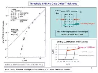
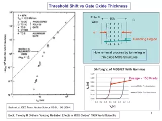
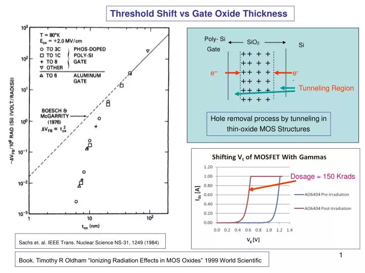
Threshold Shift vs Gate Oxide Thickness. Poly- Si Gate. SiO 2. Si. +. +. +. +. +. +. +. +. +. +. +. +. e --. e --. +. +. +. +. +. +. +. +. Tunneling Region. +. +. +. +. Hole removal process by tunneling in thin-oxide MOS Structures. Dosage = 150 Krads.

E N D
Threshold Shift vs Gate Oxide Thickness Poly- Si Gate SiO2 Si + + + + + + + + + + + + e-- e-- + + + + + + + + Tunneling Region + + + + Hole removal process by tunneling in thin-oxide MOS Structures Dosage = 150 Krads Sachs et. al. IEEE Trans. Nuclear Science NS-31, 1249 (1984) Book. Timothy R Oldham “Ionizing Radiation Effects in MOS Oxides” 1999 World Scientific
CERN ASICs Mantra: Deep sub micron is more rad hard Why ?
Can We Have High Radiation Tolerance & Higher Voltage Together ??? Controller : Low Voltage High Voltage: Switches – LDMOS, Drain Extension, Deep Diffusion etc >> 20 Volts HEMT GaN on Silicon, Silicon Carbide, Sapphire
Thin Oxide Devices (non IBM) Necessary condition for Radiation Hardness - Thin Gate Oxide But not sufficient IHP: Epi free, High resistivity substrate, Higher voltage, lower noise devices Dongbu: Epi process on substrate, lower voltage due to hot carriers in gate oxide
Fig. 4 XYSemi LDMOS Device: Effect of 60Co Gamma radiation followed by neutron radiation on VG versus ID on the same device. Fig. 5 XYSemi LDMOS Device: Effect of 1015/ cm2 of 800 MeV protons on VG versus ID. Note that shift is in opposite polarity from the expected shift normal to ionizing radiation effects.
LDMOS Structure Laterally Diffused Drain Extension High Voltage / high Frequency Main market. Cellular base stations High performance RF LDMOS transistors with 5 nm gate oxide in a 0.25 μm SiGe:C BiCMOS technology: IHP Microelectronics Electron Devices Meeting, 2001. IEDM Technical Digest. International2-5 Dec. 2001 Page(s):40.4.1 - 40.4.4
R. Sorge et al , IHP Proceedings of SIRF 2008 Conference High Voltage Complementary Epi Free LDMOS Module with 70 V PLDMOS for a 0.25 μm SiGe:C BiCMOS Platform
Non- Synchronous Replacement for LHC4913: LHC Radiation Hard LDO Made by ST Microelectronics Use with Ferrite Coil Engineering Samples 1Q2010
Bias during Radiation Max operating V & I Limit Power by duty cycle Pomona Box 30 m Power Supply V out = 20 Volts ~ 0.070 Amps 330 2 Watts 1 Ω DMM DC mV Reading = ~ 0.035 Amps @ 50% Duty Cycle Source Drain FET Pulse Generator 0.1 – 2 MHz 50 % Duty Cycle 0 to - 5 V Gate 100 . 50 Ω Terminator 2 Shorted FETs Rad vs wo Bias S Powered FET D GND G Satish Dhawan, Yale University FET Setup for Proton Radiation Exposure July 28. 2009