Download
1 / 12
130 likes | 411 Views
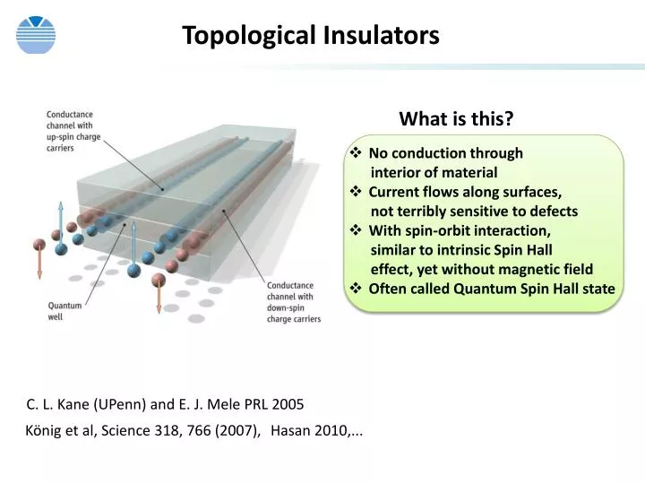
Topological Insulators. What is this?. No conduction through interior of material Current flows along surfaces, not terribly sensitive to defects With spin-orbit interaction, similar to intrinsic S pin Hall effect, yet without magnetic field

E N D
Topological Insulators What is this? • No conduction through • interior of material • Current flows along surfaces, • not terribly sensitive to defects • With spin-orbit interaction, • similar to intrinsic Spin Hall • effect, yet without magnetic field • Often called Quantum Spin Hall state C. L. Kane (UPenn) and E. J. Mele PRL 2005 König et al, Science 318, 766 (2007), Hasan 2010,...
Topological Insulators: Features and requirements There are still many misconceptions around. Here some important facts: • Single-electron effect and therefore sensitive to chemistry • Edge states in the gap occur independently of dimensionality • The basic effect is independent of spin and spin-orbit interaction • Effect is very common but not within fundamental gap • Interesting cases require inverted band structure (overlapping s & p-bands) • The effect requires sufficient distance between the material‘s boundaries
„Topological“ example: defect levels in polyacetylene (CH)x Short-Long-… Long-Short-… p* p* C-p C-p p p Bound state in gap center
1-D Tight Binding model of Topological Insulators … … p p p s s s p p s s Inverted band structure: Small s-p energy separation Normal band structure: Large s-p energy separation Tss s s p p Tpp Semiconductor Metal
1-D Tight Binding model of Topological Insulators … … p p p s s s p p s s Inverted band structure: NN-coupling opens gap and … Normal band structure: NN-coupling has little effect Tsp Tsp Tss s s p p Tpp Semiconductor Semiconductor
1-D Tight Binding model of Topological Insulators Inverted band structure: … and boundary produces states in the gap Normal band structure: NN-coupling has little effect p p s s s p p s Tsp Tsp Tpp p p s s Tss Semiconductor Semiconductor
1-D Tight Binding model of Topological Insulators p p s s s p p s Tsp Tsp Inverted band structure: Band gap opens + 2 bound states NN-coupling has no effect on boundary since y = 0. Leads to gap states ! Semiconductor with gap states
2D topological insulator HgxCd1-xTe:HgTe:HgxCd1-xTe Cartoon - without spin-orbit interaction Quantum Wire HgTe Bulk HgTe zero-gap 2-DEG HgTe Gate Gate lh e Fermi Energy hh hh e lh k3D k2D k1D Overlapping bands produce HOMO-LUMO gap Edges produce bound states in gap
2D topological insulator HgxCd1-xTe:HgTe:HgxCd1-xTe Cartoon - with spin-orbit interaction • Spin-orbit interaction adds another twist for the edge states in the gap: • Spin-up and spin-down edge states within the gap get split • For k1D > 0, only spin-up/spin-down electrons can propagate in right/left channel Spin-orbit resolved gap states E left- left- right- right- k1D
2D topological insulator HgxCd1-xTe:HgTe:HgxCd1-xTe Relativistic 4-band Envelope Function Calculations • Barrier Hg.3Cd.7Te • HgTe quantum well thickness 7.8 nm • Carrier density ~ 1×1011 cm-2 • HgTe quantum wire width 240 nm Gate Gate Band structure E(k1D) Spin-split band states (k-linear spin-orbit splitting, occurs in all ZnS semiconductors) Spin-split gap states (comes with inverted band structure)
2D topological insulator HgxCd1-xTe:HgTe:HgxCd1-xTe Relativistic 4-band Envelope Function Calculations Spin Polarization across Quantum Wire 0 Gate Gate ±V
NEGF Application: All-Electric Spin Analyzer based on Inverse Quantum Spin Hall Effect • HgTe 2DEG • T = 100 mK • VDS = 100 mV • DVgate = 18 mV QSH Normal conducting QSH Spin Density Resulting V: 8 mV Proposal by H. Buhmann