Download
1 / 1
10 likes | 140 Views
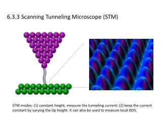
c oaxial connector. sapphire resonator. coax-to waveguide adaptor. slit. sapphire transducer. air-gap. tuning screw. SMA connector. Probe design. Abstract

E N D
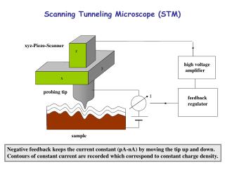
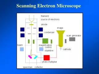
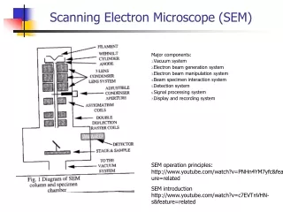
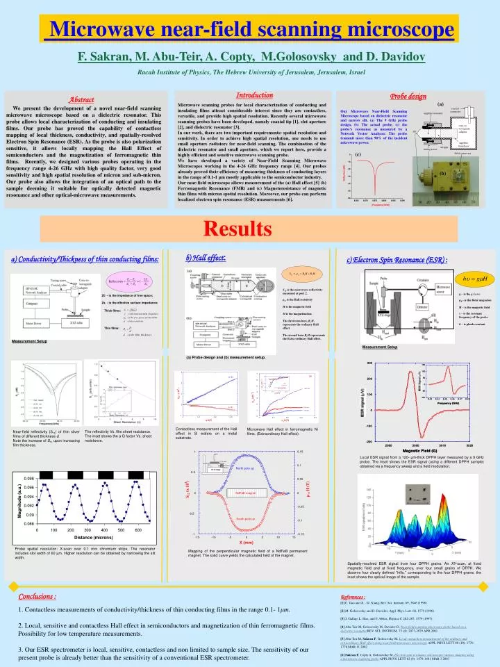
coaxial connector sapphire resonator coax-to waveguide adaptor slit sapphire transducer air-gap tuning screw SMA connector Probe design Abstract We present the development of a novel near-field scanning microwave microscope based on a dielectric resonator. This probe allows local characterization of conducting and insulating films. Our probe has proved the capability of contactless mapping of local thickness, conductivity, and spatially-resolved Electron Spin Resonance (ESR). As the probe is also polarization sensitive, it allows locally mapping the Hall Effect of semiconductors and the magnetization of ferromagnetic thin films. Recently, we designed various probes operating in the frequency range 4-26 GHz with high quality factor, very good sensitivity and high spatial resolution of micron and sub-micron. Our probe also allows the integration of an optical path to the sample deeming it suitable for optically detected magnetic resonance and other optical-microwave measurements. (a) Our Microwave Near-Field Scanning Microscope based on dielectric resonator and narrow slit. (a) The 9 GHz probe design, (b) The actual probe, (c) the probe’s resonance as measured by a Network Vector Analyzer. The probe transmit more than 90% of the incident microwave power. (c) (b) The reflectivity Vs. film sheet resistance. The inset shows the a Q factor Vs. sheet resistance. Near-field reflectivity (S11) of thin silver films of different thickness d. Note the increase of S11 upon increasing film thickness. Probe 2” Si wafer S N Permanent Magnet XYZ stage 10 mm Spatially-resolved ESR signal from four DPPH grains. An XY-scan, at fixed magnetic field and at fixed frequency, over four small grains of DPPH. We observe four clearly defined ‘‘hills,’’ corresponding to the four DPPH grains. the inset shows the optical image of the sample. Microwave near-field scanning microscope F. Sakran, M. Abu-Teir, A. Copty, M.Golosovsky and D. Davidov Racah Institute of Physics, The Hebrew University of Jerusalem, Jerusalem, Israel Introduction Microwave scanning probes for local characterization of conducting and insulating films attract considerable interest since they are contactless, versatile, and provide high spatial resolution. Recently several microwave scanning probes have been developed, namely coaxial tip [1], slot aperture [2], and dielectric resonator [3]. In our work, there are two important requirements: spatial resolution and sensitivity. In order to achieve high spatial resolution, one needs to use small aperture radiators for near-field scanning. The combination of the dielectric resonator and small aperture, which we report here, provide a highly efficient and sensitive microwave scanning probe. We have developed a variety of Near-Field Scanning Microwave Microscopes working in the 4-26 GHz frequency range [4]. Our probes already proved their efficiency of measuring thickness of conducting layers in the range of 0.1-1 μm mostly applicable to the semiconductor industry. Our near-field microscope allows measurement of the (a) Hall effect [5] (b) Ferromagnetic Resonance (FMR) and (c) Magnetoresistance of magnetic thin films with micron spatial resolution. Moreover, our probe can perform localized electron spin resonance (ESR) measurements [6]. Results b) Hall effect: a) Conductivity/Thickness of thin conducting films: c) Electron Spin Resonance (ESR) : S12 is the microwave reflectivity measured at port 2. ρxyis the Hall resistivity H is the magnetic field M is the magnetization. The first term here, RoH, represents the ordinary Hall effect. The second term ReH represaents the Extra ordinary Hall effect. g – is theg-factor μB- is the Bohr magneton H – is the magnetic field ν – is the resonant frequency of the probe h – isplank constant Z0 - is the impedance of free space; Zs - is the effective surface impedance; Thick films: Thin films: Measurement Setup Measurement Setup (a) Probe design and (b) measurement setup. Contactless measurement of the Hall effect in Si wafers on a metal substrate. Microwave Hall effect in ferromagnetic Ni films. (Extraordinary Hall effect) Local ESR signal from a 120- μm-thick DPPH layer measured by a 9 GHz probe. The inset shows the ESR signal (using a different DPPH sample) obtained via a frequency sweep and a field modulation. Probe spatial resolution: X-scan over 0.1 mm chromium strips. The resonator includes slot width of 60 µm. Higher resolution can be obtained by narrowing the slit width. Mapping of the perpendicular magnetic field of a NdFeB permanent magnet. The solid curve yields the calculated field of the magnet. Conclusions : 1. Contactless measurements of conductivity/thickness of thin conducting films in the range 0.1- 1μm. 2. Local, sensitive and contactless Hall effectin semiconductors and magnetization of thin ferromagnetic films. Possibility for low temperature measurements. 3. Our ESR spectrometer is local, sensitive, contactless and non limited to sample size. The sensitivity of our present probe is already better than the sensitivity of a conventional ESR spectrometer. References : [1] C. Gao and X. –D. Xiang, Rev. Sci. Instrum. 69, 3846 (1998) [2] M. Golosovsky and D. Davidov, Appl. Phys. Lett. 68, 1579 (1996) [3] J. Gallop, L. Hao, and F. Abbas, Physica C 282-287, 1579 (1997) [4] Abu-Teir M, Golosovsky M, Davidov D, Near-field scanning microwave probe based on a dielectric resonator,REV. SCI. INSTRUM. 72 (4): 2073-2079 APR 2001 [5] Abu-Teir M, Sakran F, Golosovsky M, Local contactless measurement of the ordinary and extraordinary Hall effect using near-field microwave microscopyAPPL PHYS LETT 80 (10): 1776-1778 MAR 11 2002 [6]Sakran F, Copty A, Golosovsky M, Electron spin resonance microscopic surface imaging using a microwave scanning probe APPL PHYS LETT 82 (9): 1479-1481 MAR 3 2003