Download
1 / 36
360 likes | 365 Views
ECE 448: Spring 2013 Lab 4 FPGA Design Flow Based on Xilinx ISE and ISim. Agenda for today. Part 1: Introduction to FPGA Design Flow based on Xilinx ISE Part 2: Seven Segment Displays Part 3: User Constraints File Part 4: Single-Step Mode & Run Mode

E N D
ECE 448: Spring 2013 Lab 4 FPGA Design Flow Based on Xilinx ISE and ISim
Agenda for today Part 1: Introduction to FPGA Design Flow based on Xilinx ISE Part 2: Seven Segment Displays Part 3: User Constraints File Part 4: Single-Step Mode & Run Mode Part 5: Digital Clock Managers and Variable Clock Frequency Part 6: Introduction to Lab 4
Part 1 Hands-on Session on FPGA Design Flow based on Xilinx ISE and Xilinx ISim
Part 2 Seven Segment Displays
Part 3 User Constraint File (UCF)
User Constraint File (UCF) • File contains various constraints for Xilinx • Clock Period • Circuit Locations • Pin Locations • Every pin in the top-level unit needs to have a pin in the UCF
Top-Level Unit for Lab 4, Tasks 5 & 6 entity lab4 is port( CLOCK : in std_logic; BTNL : in std_logic; BTNR : in std_logic; BTNU : in std_logic; BTNS : in std_logic; BTND : in std_logic; SW : in std_logic_vector(7 downto 0); LED : out std_logic_vector(7 downto 0); SEG : out std_logic_vector(6 downto 0); AN : out std_logic_vector(3 downto 0)); ); end entity lab4;
User Constraint File (UCF) - LEDs # LEDs NET "LED<0>" LOC = "U16" | IOSTANDARD = "LVCMOS33"; NET "LED<1>" LOC = "V16" | IOSTANDARD = "LVCMOS33"; NET "LED<2>" LOC = "U15" | IOSTANDARD = "LVCMOS33"; NET "LED<3>" LOC = "V15" | IOSTANDARD = "LVCMOS33"; NET "LED<4>" LOC = "M11" | IOSTANDARD = "LVCMOS33"; NET "LED<5>" LOC = "N11" | IOSTANDARD = "LVCMOS33"; NET "LED<6>" LOC = "R11" | IOSTANDARD = "LVCMOS33"; NET "LED<7>" LOC = "T11" | IOSTANDARD = "LVCMOS33";
User Constraint File (UCF) - SSD # Seven Segment Displays NET "SEG<0>" LOC = "T17" | IOSTANDARD = "LVCMOS33"; NET "SEG<1>" LOC = "T18" | IOSTANDARD = "LVCMOS33"; NET "SEG<2>" LOC = "U17" | IOSTANDARD = "LVCMOS33"; NET "SEG<3>" LOC = "U18" | IOSTANDARD = "LVCMOS33"; NET "SEG<4>" LOC = "M14" | IOSTANDARD = "LVCMOS33"; NET "SEG<5>" LOC = "N14" | IOSTANDARD = "LVCMOS33"; NET "SEG<6>" LOC = "L14" | IOSTANDARD = "LVCMOS33"; NET "AN<0>" LOC = "N16" | IOSTANDARD = "LVCMOS33"; NET "AN<1>" LOC = "N15" | IOSTANDARD = "LVCMOS33"; NET "AN<2>" LOC = "P18" | IOSTANDARD = "LVCMOS33"; NET "AN<3>" LOC = "P17" | IOSTANDARD = "LVCMOS33";
User Constraint File (UCF) Switches # Switches NET "SW<0>" LOC = "T10" | IOSTANDARD = "LVCMOS33"; NET "SW<1>" LOC = "T9" | IOSTANDARD = "LVCMOS33"; NET "SW<2>" LOC = "V9" | IOSTANDARD = "LVCMOS33"; NET "SW<3>" LOC = "M8" | IOSTANDARD = "LVCMOS33"; NET "SW<4>" LOC = "N8" | IOSTANDARD = "LVCMOS33"; NET "SW<5>" LOC = "U8" | IOSTANDARD = "LVCMOS33"; NET "SW<6>" LOC = "V8" | IOSTANDARD = "LVCMOS33"; NET "SW<7>" LOC = "T5" | IOSTANDARD = "LVCMOS33";
User Constraint File (UCF) Buttons # Buttons NET "BTNS" LOC = "B8" | IOSTANDARD = "LVCMOS33"; BTNS NET "BTNU" LOC = "A8" | IOSTANDARD = "LVCMOS33"; BTNU NET "BTNL" LOC = "C4" | IOSTANDARD = "LVCMOS33"; BTNL NET "BTND" LOC = "C9" | IOSTANDARD = "LVCMOS33"; BTND NET "BTNR" LOC = "D9" | IOSTANDARD = "LVCMOS33"; BTNR
User Constraint File (UCF) CLOCK # Buttons NET "CLOCK" LOC = "V10" | IOSTANDARD = "LVCMOS33";
Part 4 Single Step Mode & Run Mode
step run loadA IVA loadB IVB loadA loadB 8 8 OR cnz en en nexti nexto nexti ld ld OR OR LFSR LFSR clk clk rst rst rst rst clk clk AND not done AND X”00” X”00” 8 8 en CNTR UP nexto 0 0 1 1 rst rst cnz cnz clk clk 8 8 k 10 A B = X”3FF” 10 k9..8 sel 2 8 done k7..0 LAB2 ≠ 0 En ‘0’ cnz X Y 8 8 en nexto en nexto rst rst rst MISR rst MISR clk clk clk clk 8 8 XSGN YSGN
Generation of Step & Next Using Buttons rst rst rst clk clk clk BTNU step Debouncer RED rst run rst ‘1’ Q D BTNS en Debouncer RED clk clk RED = Rising Edge Detector
Part 5 Digital Clock Managers and Variable Clock Frequency
Clock Management • Clock sources are generated off of the FPGA • Clock source needs to enter the FPGA • Clock needs to be “de-jittered” • Clock naturally has non-constant duty cycle and period • Clock needs to reach the rest of the chip
Clock Management • Ideal clock has one frequency • Clock jitter is the undesired deviation in the timing of clock edges • We can see the jitter in the top (yellow) trace • Blue clock is de-jittered
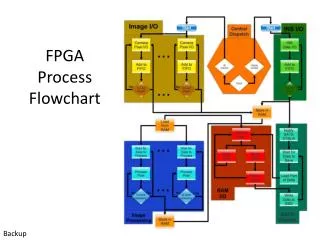
Clock Management ‘0’ clkfx_obufg clkFX DCM_SP BUFG 0 clkfx clk • CLOCK Enters FPGA and enters IBUFG • Output of BUFGMUX goes to the rest of the FPGA • Invert of LOCKED signal is used as a reset for the top-level circuit • To simulate, include the following lines in the library section • library UNISIM; • use UNISIM.vcomponents.all; clk_ibufg clk0_obufg clk100 IBUFG CLOCK clkin clk0 BUFG 1 BUFGMUX BTNL rst_or rst BTNR rst clkfb locked
Digital Clock Manager • DCM can also change clock frequency • CLK2X doubles frequency • CLKDV and CLKFX change the frequency based on the generics (see instantiation)
DCM_SP Instantiation (1) DCM_SP_inst : DCM_SP generic map ( CLKDV_DIVIDE => 2.0, -- CLKDV divide value -- (1.5,2,2.5,3,3.5,4,4.5,5,5.5,6,6.5,7,7.5,8,9,10,11,12,13,14,15,16). -- Divide value on CLKFX outputs - D - (1-32) -- Multiply value on CLKFX outputs - M - (2-32) -- CLKIN divide by two (TRUE/FALSE) -- Input clock period specified in nS -- Output phase shift (NONE, FIXED, VARIABLE) -- Feedback source (NONE, 1X, 2X) CLKFX_DIVIDE => …………., CLKFX_MULTIPLY => ………, CLKIN_DIVIDE_BY_2 => FALSE, CLKIN_PERIOD => 10.0, CLKOUT_PHASE_SHIFT => "NONE", CLK_FEEDBACK => "1X”,
DCM_SP Instantiation (2) -- SYSTEM_SYNCHRNOUS or SOURCE_SYNCHRONOUS DESKEW_ADJUST => "SYSTEM_SYNCHRONOUS", -- Unsupported generics - Do not change value DFS_FREQUENCY_MODE => "LOW", DLL_FREQUENCY_MODE => "LOW", DSS_MODE => "NONE", DUTY_CYCLE_CORRECTION => TRUE, FACTORY_JF => X"c080", PHASE_SHIFT => 0, STARTUP_WAIT => FALSE -- Amount of fixed phase shift (-255 to 255) PHASE_SHIFT => 0, -- Delay config DONE until DCM_SP LOCKED (TRUE/FALSE) STARTUP_WAIT => FALSE )
DCM_SP Instantiation (3) port map ( CLK0 => …………., -- 0 degree clock output CLK180 => open, -- 180 degree clock output CLK270 => open, -- 270 degree clock output CLK2X => open, -- 2X clock frequency clock output CLK2X180 => open, -- 2X clock frequency 180 degree clock output CLK90 => open, -- 90 degree clock output CLKDV => open, -- Divided clock output CLKFX => …………, -- Digital Frequency Synthesizer (DFS) output CLKFX180 => open, -- 180 degree CLKFX output LOCKED => …………, -- DCM_SP Lock Output
DCM_SP Instantiation (4) PSDONE => open, -- Phase shift done output STATUS => open, -- DCM_SP status output CLKFB => …………., -- Clock feedback input CLKIN => ………….., -- Clock input DSSEN => ‘0’, -- Unsupported, specify to GND PSCLK => clk_ibufg, -- Phase shift clock input PSEN => ‘0’, -- Phase shift enable PSINCDEC => ‘0’ , -- Phase shift increment/decrement input RST => ………… -- Active high reset input );
Library and Package In order to compile, simulate and synthesize a circuit including DCM_SP, you need to include in the top-level circuit: library UNISIM; use UNISIM.vcomponents.all;
Clock Buffers IBUFG_inst : IBUFG generic map ( IOSTANDARD => "DEFAULT") port map ( O => O, I => I); • Dedicated clock route for reaching a DCM and the rest of the chip • Should be used for a clock port BUFG_inst : BUFG port map ( O => O, I => I); • Dedicated clock route for reaching the rest of the chip at the same time • Should be used for all generated clocks • Output from DCM • Output from clock divider circuits
Clock Multiplexer BUFGMUX_inst : BUFGMUX generic map ( CLK_SEL_TYPE => "SYNC" -- Glitchles ("SYNC") or fast ("ASYNC") clock switch-over ) port map ( O => …….., -- 1-bit output: Clock buffer output I0 => …….., -- 1-bit input: Clock buffer input (S=0) I1 => …….., -- 1-bit input: Clock buffer input (S=1) S => ……… -- 1-bit input: Clock buffer select );
Part 6 Introduction to Lab 4