Download

1 / 22
410 likes | 967 Views
The Xilinx Spartan 3 FPGA. EGRE 631 2/2/09. Basic types of FPGA’s. One time programmable Reprogrammable (non-volatile) Retains program when powered down SRAM-based reprogramable Must be reprogrammed each time powered up This is usually accomplished by using a small serial PROM.

E N D
The Xilinx Spartan 3 FPGA EGRE 631 2/2/09
Basic types of FPGA’s • One time programmable • Reprogrammable (non-volatile) • Retains program when powered down • SRAM-based reprogramable • Must be reprogrammed each time powered up • This is usually accomplished by using a small serial PROM.
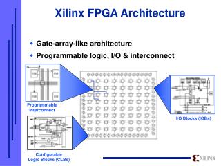
Spartan-3 ArchitectureFundamental Elements • Configurable Logic Blocks (CLBs) • Consists of RAM based look up table to implement logic and storage elements that can be used as flip-flops or latches. • Input Output Blocks (IOBs) • Controls the flow of data between IO pins and internal logic. Supports many different signal standards. (Tri-state, bidirectional, LVTTL, etc. • Block RAM (BRAM) • 18 bit Multiplier Blocks • Digital Clock Manager (DCM)
Spartan 3 Configurable Logic Blocks (CLB’s) • CLBs contain Ram based lookup tables to implement logic and storage elements that can be used as flip-flops or latches. • CLBs can be programmed to perform a wide variety of logic functions as well as store data.
Spartan 3E IO Blocks (IOB’s) • IOB’s control flow of data between IO pins and the internal logic. • Each IOB supports bidirectional data flow, 3-state operation, and numerous different signal standards. (We will typically use LVTTL). See data sheet.
BUFT BUF T Slices and CLBs COUT COUT Switch Matrix • Each Spartan-III CLB contains four slices • Local routing provides feedback between slices in the same CLB, and it provides routing to neighboring CLBs • A switch matrix provides access to general routing resources Slice S3 Slice S2 SHIFT Slice S1 Slice S0 Local Routing CIN CIN
Simplified Slice Structure • Each slice has four outputs • Two registered outputs, two non-registered outputs • Two BUFTs associated with each CLB, accessible by all 16 CLB outputs • Carry logic runs vertically, up only • Two independent carry chains per CLB Slice 0 LUT PRE Carry D Q CE CLR LUT Carry PRE D Q CE CLR
Detailed Slice Structure • The next few slides discuss the slice features • LUTs • MUXF5, MUXF6, MUXF7, MUXF8 (only the F5 and F6 MUX are shown in this diagram) • Carry Logic • MULT_ANDs • Sequential Elements
Combinatorial Logic A B Z C D Look-Up Tables • Combinatorial logic is stored in Look-Up Tables (LUTs) • Also called Function Generators (FGs) • Capacity is limited by the number of inputs, not by the complexity • Delay through the LUT is constant
F8 F5 F6 F5 F7 F5 F6 F5 Connecting Look-Up Tables MUXF8 combines the two MUXF7 outputs (from the CLB above or below) CLB Slice S3 MUXF6 combines slices S2 and S3 Slice S2 MUXF7 combines the two MUXF6 outputs Slice S1 MUXF6 combines slices S0 and S1 Slice S0 MUXF5 combines LUTs in each slice
COUT COUT To S0 of the next CLB To CIN of S2 of the next CLB SLICE S3 First Carry Chain CIN COUT SLICE S2 SLICE S1 CIN Second Carry Chain COUT SLICE S0 CIN CIN CLB Fast Carry Logic • Simple, fast, and complete arithmetic Logic • Dedicated XOR gate for single-level sum completion • Uses dedicated routing resources • All synthesis tools can infer carry logic
MULT_AND Gate • Highly efficient multiply and add implementation • Earlier FPGA architectures require two LUTs per bit to perform the multiplication and addition • The MULT_AND gate enables an area reduction by performing the multiply and the add in one LUT per bit LUT A CY_MUX CO S DI CI CY_XOR MULT_AND A x B LUT B LUT
Distributed SelectRAM Resources RAM16X1S D • Uses a LUT in a slice as memory • Synchronous write • Asynchronous read • Accompanying flip-flops can be used to create synchronous read • RAM and ROM are initialized duringconfiguration • Data can be written to RAMafter configuration • Emulated dual-port RAM • One read/write port • One read-only port LUT WE WCLK A0 O A1 A2 A3 RAM32X1S RAM16X1D D D WE WE Slice WCLK WCLK A0 O A0 SPO LUT A1 A1 A2 A2 A3 A3 A4 DPRA0 DPO DPRA1 DPRA2 LUT DPRA3
Block SelectRAM Resources 18-kb block SelectRAM memory • Up to 3.5 Mb of RAM in 18-kb blocks • Synchronous read and write • True dual-port memory • Each port has synchronous read and write capability • Different clocks for each port • Supports initial values • Synchronous reset on output latches • Supports parity bits • One parity bit per eight data bits DIA DIPA ADDRA WEA ENA SSRA DOA CLKA DOPA DIB DIPB ADDRB WEB ENB SSRB DOB CLKB DOPB
Dedicated Multiplier Blocks • 18-bit twos complement signed operation • Optimized to implement Multiply and Accumulate functions • Multipliers are physically located next to block SelectRAM™ memory 18 x 18 Multiplier Data_A (18 bits) Output (36 bits) Data_B (18 bits)
Spartan-3A FPGA Starter Kit board User Guide Spartan III Starter –Kit