Download
1 / 12
120 likes | 304 Views
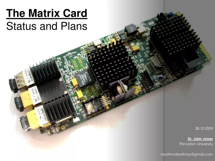
TBD. The Matrix Card Status and Plans. 28.10.2009 Dr. John Jones Princeton University neutrinodeathray@gmail.com. The Matrix Processor - Schematic. SNAP12. 2Gb DDR2. Mindspeed 72x72 Cross-point Switch. Xilinx Virtex 5 FPGA (LX110T). POP4. 3U μ TCA I/O (20/20).

E N D
TBD The Matrix Card Status and Plans 28.10.2009 Dr. John Jones Princeton University neutrinodeathray@gmail.com
The Matrix Processor - Schematic SNAP12 2Gb DDR2 Mindspeed 72x72 Cross-point Switch Xilinx Virtex 5 FPGA (LX110T) POP4 3U μTCA I/O (20/20) OPTICAL I/O (16/16) 2Gb DDR2 SNAP12 NXP 2366 μC Dr. John Jones (neutrinodeathray@gmail.com)
The Matrix Processor – Top Photo FPGA MTP Optics Ethernet Mindspeed Switch Dr. John Jones (neutrinodeathray@gmail.com)
The Matrix Processor – Bottom Photo NXP Microcontroller DDR2 SDRAM TCA Connector Dr. John Jones (neutrinodeathray@gmail.com)
Prototype Tests The original Matrix Card design had a number of (mostly minor) faults: Microcontroller was too small for firmware Some TX serial links showed signal degradation (plane structure issue?) Missing pull-up / series-termination resistors Tests included: All serial links (internal loopback, fiber loopback – 16 links) GbE over backplane (1 link) GbE over fiber (1 link) uC control & programming CPLD JTAG switching DDR2 RAM Inter-Matrix card testing (16 links) Dr. John Jones (neutrinodeathray@gmail.com)
Serial Link Issues - Before Serial Power Dr. John Jones (neutrinodeathray@gmail.com)
Serial Link Issues - Detail Before After Dr. John Jones (neutrinodeathray@gmail.com)
Rev. A Tests All outstanding issues regarding prototype were fixed in Rev. A board. Two Rev. A boards (one LANL, one CERN) Two prototype boards (one LANL, one CERN) All TX/RX channels are now stable at 3.75Gb/s over fiber. Design is now ready for production. Dr. John Jones (neutrinodeathray@gmail.com)
Lessons Learned The Matrix card is an extremely dense / complex board The manufacturer even showed it to a large well-known network company. They had never made one with as many serial links at such high density… For our field, such aggressive increases in density are necessary... ...but the problems (in particular the transmitter degradation issue) were non-trivial to solve and are hard to model It is more important than ever to have as few, well-understood pieces of hardware in the upgrade as possible... Put another way, FPGAs are complicated enough on their own that it’s best not to spend all our time debugging new hardware. Dr. John Jones (neutrinodeathray@gmail.com)
Reference Design Availability The Matrix Card was intended to be a common hardware platform For that to happen, the design must be made readily available The Open Hardware Repository (OHR, Javier Serrano, CERN) was conceived to create common hardware platforms that could be shared for future development Design is made available in full (reference schematics, gerbers, etc…) As part of the process, the design is reviewed and tested by many groups Increased reliability Shared knowledge The Matrix card design will soon (if not already) be available IN FULL on the OHR (www.ohwr.org) Dr. John Jones (neutrinodeathray@gmail.com)
Matrix Card Production Run If you don’t want to build one yourself… We are currently planning for a production run of ~20 Matrix cards, available for use within the next 6 months Interested groups should contact C. Foudas These will be used in concert with the Mini-T card (Greg Iles – IC) as our first development platform for future triggers Spare cards from this run will available for purchase Allow groups with limited access to engineering facilities to use them for algorithm development Microcontroller firmware will be pre-installed for programming the FPGA & basic communication An example bitstream will also be provided Example UDP/IP core can also be provided on request Dr. John Jones (neutrinodeathray@gmail.com)
MINI-T5 2x 40 Diff Pairs at 1.25 Gb/s Low latency interface Atmel AT32UC3A 2x QSFP 4 BiDir 5.0 Gb/s 8 Backplane (LVDS option) 2x SNAP12-OUT 12 x 5.0 Gb/s Xilinx XC5VLXT150T 2x SNAP12-IN 12 x 5.0 Gb/s Manufacture September


![Team #TBD Member1, Member2, Member3, Member4 [Alphabetical]](https://cdn5.slideserve.com/9674933/team-tbd-member1-member2-member3-member4-alphabetical-dt.jpg)