Download
1 / 44
440 likes | 570 Views
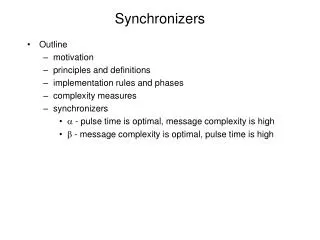
SoC Clock Synchronizers Project. Progress Presentation. D0827. Students: Elihai Maicas Harel Mechlovich. Instructor: Shlomi Beer-Gingold. Presentation Agenda. General project description Technical specifications Background Architecture and HW needs Software Timeline.

E N D
SoC Clock Synchronizers Project Progress Presentation D0827 Students: Elihai Maicas Harel Mechlovich Instructor: Shlomi Beer-Gingold
Presentation Agenda • General project description • Technical specifications • Background • Architecture and HW needs • Software • Timeline
Project Description • Explore and understand the synchronization issue • Articles • Literature • Brain storming • Implementation of several synchronizers • Plesiochronous • Periodic • Asynchronous
Project Description • Testing of the synchronizers • Correctness • Compare between the different solutions while looking at: • Latency • Area • Power • Simplicity • Plug-n-play
Project Description • Conclusions • Which solutions are preferred • When to use what • Pros and Cons • Limitations • Possible new suggestions
Spec • XUPV2P board (xillinx Spartan 2)
Spec • DLP mini-board • The DLP-USB245M provides an easy cost-effective method of transferring data to / from a peripheral and a host at up to 8 Million bits (1-Megabyte) per second. Its simple FIFO-like design makes it easy to interface to any microcontroller or microprocessor via IO ports • Signal generator
Background • We consider the project to be a part of the continuous research of the synchronization problem and its solutions • Our findings and final conclusions could be used for helping future projects in the HS DSL and other laboratories • Future projects can examine other solutions and/or look further into the same solutions from the point we left them
Background • The process of deciding which solutions (synchronizers) included reading articles and other literature • Parameters that were taken into account: • Existing knowledge • Matching class • Complexity • Possible uses • Frequentness
Selected Solutions • The project will cover 5 selected synchronizers • The synchronizers match 3 different synchronization classes: • Plesiochronous • FIFO Synchronizer with Multisynchronous Support • Two-Register Synchronizer with Conflict Detector • Periodic • Two-Register Synchronizer with Conflict Detector and Predictor • Asynchronous • Two-Flop (AKA Brute-Force) Synchronizer • General Purpose Asynchronous FIFO Synchronizer
Selected Solutions • FIFO Synchronizer with Multisynchronous Support • Flow Control • Data is inserted into the FIFO buffer with the transmitter clock, xclk • Data is removed from the FIFO buffer with the receiver clock rclk Plesiochronous
Selected Solutions • Receive pointer rp is periodically updatedby synchronizing the transmit pointer xp to the receiver clock rclk • rp is replaced with the previous xpwhenever the control signal resync is high • rp is incremented normally whenever resync is low • resync signal is driven by a controller which is designed to activate a resynchronization cycle whenever the phase difference between xclk and rclk wraps • These updating events keep the counters in a correct phase, but lead to data dropping or replication • Data-rate mismatch problem is handled by inserting null symbols into the data stream • Open-loop approach • Closed-loop approach Plesiochronous
Selected Solutions • Pointer controller Plesiochronous
Selected Solutions • Latency • . • Does not include null injections • Pros • No chance of synchronization failure • Cons • Quite a long latency • Requires design consideration – not a plug & play device Plesiochronous
Selected Solutions • Two-Register Synchronizer with Conflict Detector Plesiochronous
Selected Solutions • Synchronizer assembled of:Conflict Detector and Two-Register Synchronizer • Flow Control • xclk transition is unsafe, if it takes place within the keep-out region of the rclk, i.e., within the aperture of the sampling flip-flop Plesiochronous
Selected Solutions • To detect this, the signal is sampled at the borders of the keep-out region: a flip-flop setup time ts before and a flip-flop hold time th after the actual sampling edge of the receiver clock • If the results are different(XOR gate) the signal is unsafe, therefore rclk will be “pushed out” of the keep-out region to avoid a sync failure • Otherwise the signal is safe and can be sampled without any time manipulation on rclk Plesiochronous
Selected Solutions • Latency • . • Pros • Delay components required only for clocks • Plug & Play • Cons • Small, but not zero, chance of sync failure • Area Plesiochronous
Two-Register Synchronizer with Conflict Detector and Clock Predictor Selected Solutions Periodic
Selected Solutions • Synchronizer assembled of:Clock Predictor, Conflict Detector and Two-Register Synchronizer • Flow Control • pxclk, a prediction of xclk, is driven intothe Conflict Detector • pxclk transition is unsafe, if it takes place within the keep-out region of the rclk, i.e., within the aperture of the sampling flip-flop Periodic
Selected Solutions • To detect this, the signal is sampled at the borders of the keep-out region: a flip-flop setup time ts before and a flip-flop hold time th after the actual sampling edge of the receiver clock • If the results are different(XOR gate) the signal is unsafe, therefore rclk will be “pushed out” of the keep-out region to avoid a sync failure • Otherwise the signal is safe and can be sampled without any time manipulation on rclk Periodic
Selected Solutions • The Clock Predictor • The circuit predicts the value of the transmitter clock, xclk, N receiver clocks (rclk) in the future • This is the phase shift , where is the cycle time of the transmitter clock. • Such a phase shift can be generated using a simple delay-locked loop Periodic
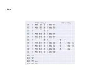
Selected Solutions • For example, let’s take the following clocks: • Now let’s delay xclk by : • You can see that the second waveform predicts the first, one receiver clock in the future • Important! For practical uses, there’s no need to delay xclk by but by , which will result the same prediction of course Periodic
Selected Solutions • Latency • . • Pros • Delay components required only for clocks • Plug & Play • Cons • Small, but not zero, chance of sync failure • Area Periodic
Selected Solutions • Two-Flop (AKA Brute-Force) Synchronizer Asynchronous
Selected Solutions • Flow Control • Synchronizes the asynchronous input A to the clock xclk • First flip-flop FF1 samples A • May go into a metastable state depending on the timing of A and xclk • Then we await the possible metastable state to end for a waiting period tw • Usually the waiting time is one clock cycle, which means that the output of FF1 is sampled by the second flip-flop FF2 to generate the final synchronized signal AS Asynchronous
Selected Solutions • In general, to implement an N-cycle waiting period, we need N casca-ded flip-flops in addition to the sampling flip-flop FF1 • Total synchronization latency is N+1 clock cycles Asynchronous
Selected Solutions • Latency • . • Pros • Easy to implement • Cons • Latency! Asynchronous
Selected Solutions • General Purpose Asynchronous FIFO Synchronizer Asynchronous
Selected Solutions • Flow Control • Data in inserted into the FIFO buffer with the transmitter clock xclk keeping the control signal shiftIn high • Data in removed from the FIFO buffer with the receiver clock rclk keeping the control signal shiftOut high • No actual synchronization delay or failures in the data path • Provides inherent flow control via the full and empty signals • when the FIFO is about to be overrun, full is asserted, and the transmitter pauses its data sending process by setting shiftIn low • when the FIFO is about to be underrun, empty is asserted, and the receiver pauses reading by setting shiftOut low
Selected Solutions • Latency • No actual synchronization delay • Pros • No delay • No failures • Cons • Extremely expansive in area • Not a plug & play device
HW Requirements • General purpose board
Test Circuit • CLK_RST – to control all clock distribution. • Periodic: We will output derivative of theinput clock with frequency difference ofdozens presents using DCM • Plesiochronous: Using two DCMs concatinated, we willcreate a second clock that have 0.1% diff from the ref clock
Test Circuit • FSMs: • Main FSM– controls the reading fromthe DRAM_SRC • Write FSM– controls which DRAM_DST gets written • Compare FSM– controls which DRAM_DST gets compared to the DRAM_SRC
Test Circuit • DRAMs: • DRAM_SRC– holds random generated data to be written to the DRAM_DST_* • DRAM_DST_*– gets written with data sourced from the DRAM_SRC • DRAM_CMP– holds the compare results
Test Circuit • Main FSM
Test Circuit • Write FSM
Test Circuit • Compare FSM
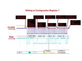
Software • Using the USB interface of the DLP, we will create a GUI through we will be able to: • configure the test registers: DUT synchronizer, transmitter and reciever clocks, “delay lines” value (configure DCM) etc. • Read back test results