Download
1 / 48
480 likes | 485 Views
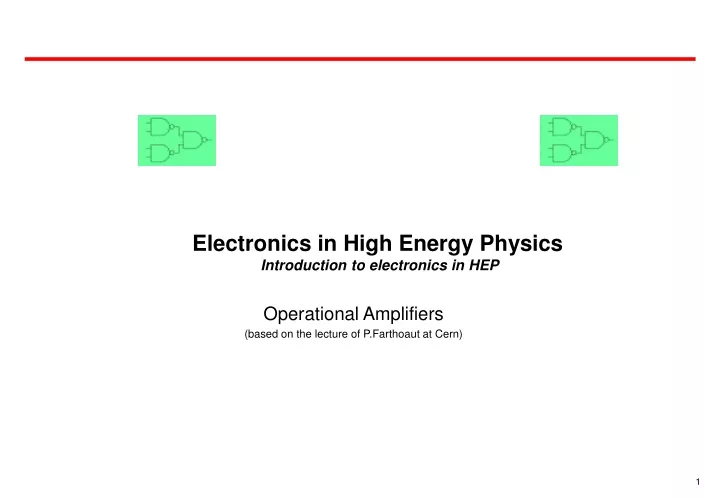
This article provides an introduction to electronics in high energy physics, focusing on operational amplifiers. Topics covered include feedback, ideal op-amp, voltage amplifier, summation and differentiation, current amplifier, charge amplifier, non-ideal amplifier, and more.

E N D
Electronics in High Energy Physics Introduction to electronics in HEP Operational Amplifiers (based on the lecture of P.Farthoaut at Cern)
Operational Amplifiers • Feedback • Ideal op-amp • Applications • Voltage amplifier (inverting and non-inverting) • Summation and differentiation • Current amplifier • Charge amplifier • Non-ideal amplifier • Offset • Bias current • Bandwidth • Slew rate • Stability • Drive of capacitive load • Data sheets • Current feedback amplifiers
y x m s e s d b Feedback • Y is a source linked to X • Y = m x • Open loop • x = d e • y = m x • s = s y = s d m x • Closed loop • m is the open loop gain • bm is the loop gain
x m s e s d b Interest of the feedback • In electronics • m is an amplifier • b is the feedback loop • d and s are input and output impedances • If m is large enough the gain is independent of the amplifier
- -A e e + Operational amplifier • Gain A very large • Input impedance very high • I.e input current = 0 • A(p) as shown
R2 I R1 - -A e e + Vout Vin How does it work? • Direct gain calculation • Feed-back equation • Ideal Op-Amp
R2 I R1 - Vout + Vin Non-inverting amplifier • Input impedance • Gain • Called a follower if R2 = 0
R2 I R1 - Vin Vout + Inverting amplifier • Gain • Input impedance • Gain error
R I R1 - V1 I1 Rn Vn In Vout + Summation • If Ri = R • Transfer function
R2 I1 R1 - V1 I1 R1 Vout + V2 I2 R2 Differentiation
C R - Iin Vout + Current-to-Voltage converter (1) • Vout = - R Iin • For high gain and high bandwidth, one has to take into account the parasitic capacitance
R1 R2 - r Iin Vout + Current-to-Voltage converter (2) • Equivalent feedback resistor = R1 + R2 + R2 * (R1/r) • ex. R1 = R2 = 100 k ; r = 1 k ; Req = 10.2 M • Allows the use of smaller resistor values with less problems of parasitic capacitance • High resistor value with small ones
R C - I Vout + Charge amplifier (1) • Requires a device to discharge the capacitor • Resistor in // • Switch
R C R2 C1 - C2 R1 V2 I V1 + Input ChargeIn a few ns Shaping a few 10’s of ns Output of the charge amplifierVery long time constant Charge amplifier (2)
C - Vin -A e e Vout + Y X X Y Z Z2 Z1 Miller effect • Charge amplifier • Vin = e • Vout = -A e • The capacitor sees a voltage (A+1) e • It behaves as if a capacitor (A+1)C was seen by the input • Miller’s theorem • Av = Vy / Vx • Two circuits are equivalent • Z1 = Z / (1 - Av) • Z2 = Z / (1-Av-1)
Common mode • The amplifier looks at the difference of the two inputs • Vout = G * (V2 - V1) • The common value is in theory ignored • V1 = V0 + v1 • V2 = V0 + v2 • In practice there are limitations • linked to the power supplies • changes in behaviour • Common mode rejection ratio CMRR • Differential Gain / Common Gain (in dB)
Ib- Zc - e Zd -A e Zout + Vd Zc Ib+ Non-ideal amplifier • Input Offset voltage Vd • Input bias currents Ib+ and Ib- • Limited gain • Input impedance • Output impedance • Common mode rejection • Noise • Bandwidth limitation & Stability
R2 I R1 - Vd Vout + Input Offset Voltage • “Zero” at the input does not give “Zero” at the output • In the inverting amplifier it acts as if an input Vd was applied • (Vout) = G Vd • Notes: • Sign unknown • Vd changes with temperature and time (aging) • Low offset = a few mV and DVd = 0.1 mV / month • Otherwise a few mV
R2 Ib- R1 - + Vout Ib+ R3 Input bias current (1) • (Vout) = R2 Ib- • (Vout) = - R3 (1-G) Ib+ • Error null forR3 = (R1//R2) if Ib+ = Ib-
C Ib- - Vout R3 + Ib+ Input bias current (2) • In the case of the charge amplifier it has to be compensated • Switch closed before the measurement and to discharge the capacitor • Values • less than 1.0 pA for JFET inputs • 10’s of nA to mA bipolar
R2 I R1 - Vc/Fr Vout + Common mode rejection • Non-inverting amplifier • Input voltage Vc/Fr (Vc common mode voltage) • Same effect as the offset voltage
R2 I R1 - -A e Vin e + Vout Gain limitation • A is of the order of 105 • Error is very small
R2 Zc- R1 - Zd + Vout Zc+ Vin Input Impedance • Zin = Zc+ // (Zd A / G) ~ Zc+ G= (R1+R2)/R1 • Non-inverting amplifier
R2 I0 + Iout R1 - Iout e I0 -A e Z0 + Vout Output impedance • Non-inverting amplifier
Maximum Output Swing R2 RL*Imax I R1 - RL + Vout Vin RL Current drive limitation • Vout = R I = RL IL • The op-amp must deliver I + IL = Vout (1/R + 1/RL) • Limitation in current drive limits output swing
f3db= fT/G fT Bandwidth • Gain amplifier of non-inverting G(p) = G A(p) / (G + A(p)) • A(p) with one pole at low frequency and -6dB/octave • A(p) = A0 / (p+w0) • G = (R1+R2)/R1 40 dB • Asymptotic plot • G < A G(p) = G • G > A G(p) = A(p)
Slew Rate • Limit of the rate at which the output can change • Typical values : a few V/ms • A sine wave of amplitude A and frequency f requires a slew rate of 2pAf • S (V/ms) = 0.3 fT (MHz); fT = frequency at which gain = 1
Settling Time • Time necessary to have the output signal within accuracy • ±x% • Depends on the bandwidth of the closed loop amplifier • f3dB = fT / G • Rough estimate • 5 t to 10 t with t = G / 2 p fT
Stability Unstable amplifier • G(p) = A(p) G / (G + A(p)) • A(p) has several poles • If G = A(p) when the phase shift is 180o then the denominator is null and the circuit is unstable • Simple criteria • On the Bode diagram G should cut A(p) with a slope difference smaller than -12dB / octave • The loop gain A(p)/G should cut the 0dB axe with a slope smaller than -12dB / octave • Phase margin • (1800 - Phase at the two previous points) • The lower G the more problems -12 dB/octave -12 dB/octave - Open loop gain A(p) - Ideal gain G - Loop gain A(p)/G
-6 dB/octave -6 dB/octave Compensation Pole in the loop Stability improvement • Move the first pole of the amplifier • Compensation • Add a pole in the feed-back • These actions reduce the bandwidth
R2 R1 - C = 20 pF 10 C Load = 0.5 mF + Capacitive load • Buffering to drive lines • The output impedance of the amplifier and the capacitive contribute to the formation of a second pole at low frequency • A’(p) = k A(p) 1/(1+r C p) with r = R0//R2//R • A(p) = A0 / (p+w0) • Capacitance in the feedback to compensate • Feedback at high frequency from the op-amp • Feedback at low frequency from the load • Typical values a few pF and a few Ohms series resistor
- -A e e + Current feedback amplifiers • Voltage feedback - Zt ie ie + • Current feedback • Zt = Vout/Ie is called the transimpedance gain of the amplifier
R2 I R1 - Zt ie ie Vout + Vin Applying Feedback • Non-inverting amplifier • Same equations as the voltage feedback
R2 I R1 - Zt ie ie Vout + Vin Frequency response • The bandwidth is not affected by the gain but only by R2 • Gain and bandwidth can be defined independently • Different from the voltage feedback • f3dB = fT / G
Data sheet of a current feedback amplifier (cont’) • Very small change of bandwidth with gain
Transmission Lines • Lossless Transmission Lines • Adaptation • Reflection • Transmission lines on PCB • Lossy Transmission Lines
Lx Cx Lx Cx Z Lossless transmission lines (1) • L,C per unit length x • Impedance of the line Z • Pure resistance
Lx Z Cx I V1 V2 Lossless transmission lines (2) • Propagation delay • Pure delay
Lossless transmission lines (3) • Characteristic impedance pure resistance • Pure delay • Capacitance and inductance per unit of length • Example 1: coaxial cable • Z = 50 W • t = 5 ns/m • L = 250 nH/m; C = 100 pF/m • Example 2: twisted pair • Z = 100 W • t = 6 ns/m • L = 600 nH/m ; C = 60 pF/m
Zs Zo Vs Is Z L V Reflection (1) • Source generator • V, Output impedance Zs • All along the line Vs = Z0 Is • If the termination resistance is ZL a reflection wave is generated to compensate the excess or lack of current in ZL • Line appears as Z0 • The reflected wave has an amplitude
ZS = 1/3 Z0 ZL = 3 Z0 ZS = 3 Z0 ZL = 3 Z0 Reflection (2) • The reflected wave travels back to source and will also generate a reflected wave if the source impedance is different from Z0 • During each travel some amplitude is lost • The reflection process stops when equilibrium is reached • VS = VL • Zs < Z0 & ZL > Z0Dumped oscillation • Zs > Z0 & ZL > Z0Integration like
Zs Zo V 1 transit time 2 transit time Vs Reflection (3) • Adaptation is always better • At the destination: no reflection at all • At the source: 1 reflection dumped • Ex. ZL = 3 Z0 • Can be used to form signal • Clamping
Transmission lines on PCB • Microstrip • Stripline
Rs L C Rp Lossy transmission lines • Idem with RsL instead of L, Rp//C instead of C • Characteristic impedance depends on w • Even Rs is a function of w because of the skin effect • Signal is distorted • Termination more complex to compensate cable characteristic
Bibliography • The Art of Electronics, Horowitz and Hill, Cambridge • Very large covering • An Analog Electronics Companion, S. Hamilton, Cambridge • Includes a lot of Spice simulation exercises • Electronics manufacturers application notes • Available on the web • (e.g. http://www.national.com/apnotes/apnotes_all_1.html) • For feedback systems and their stability • FEED-2002 from CERN Technical Training