Download
1 / 27
270 likes | 356 Views
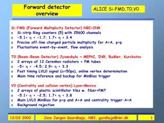
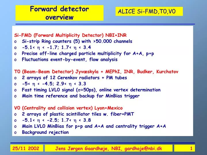
Forward detector overview. Si-FMD (Forward Multiplicity Detector) NBI+INR Si-strip Ring counters (5) with >50.000 channels -5.1< < -1.7; 1.7< < 3.4 Precise off-line charged particle multiplicity for A+A, p+p Fluctuations event-by-event, flow analysis

E N D
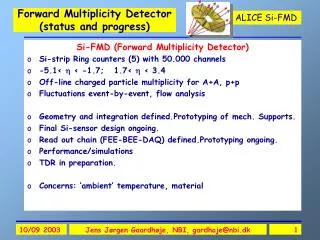
Forward detector overview Si-FMD (Forward Multiplicity Detector) NBI+INR • Si-strip Ring counters (5) with >50.000 channels • -5.1< < -1.7; 1.7< < 3.4 • Precise off-line charged particle multiplicity for A+A, p+p • Fluctuations event-by-event, flow analysis T0 (Beam-Beam Detector) Jyvæskyla + MEPhI, INR, Budker, Kurchatov • 2 arrays of 12 Cerenkov radiators + PM tubes • -5< < -4.5; 2.9< < 3.3 • Fast timing LVL0 signal (=50ps), online vertex determination • Main time reference and backup for MinBias trigger V0 (Centrality and collision vertex) Lyon+Mexico • 2 arrays of plastic scintillator tiles w. fiber+PMT • -5.1< < -2.5; 1.7< < 3.8 • Main LVL0 MinBias for p+p and A+A and centrality trigger A+A • Background rejection Jens Jørgen Gaardhøje, NBI, gardhoje@nbi.dk
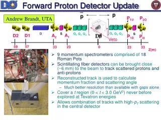
Forward detectors V01.7 < |h| < 3.8and –5.1 < | h | < -2.5 Interaction trigger, centrality trigger and beam-gas rejection. Two arrays of 72 scintillator tiles readout via fibers PMD pre-shower det. T0L T0R2.9 < |h| < 3.3 T0 for the TOF (< 50 ps time res.) Two arrays of 12 quartz counters. Also backup to V0 SI-FMD Multiplicity and dn/dh 1.7 < h < 3.4 and -5.1 < h < -1.7 Silicon pad detector disks (slow readout) Jens Jørgen Gaardhøje, NBI, gardhoje@nbi.dk
Integration in ALICE Si-1 V0-R Si-2 T0-R Si-3 Jens Jørgen Gaardhøje, NBI, gardhoje@nbi.dk
FWD detectors Jens Jørgen Gaardhøje, NBI, gardhoje@nbi.dk
CERN Maquette 1:1 ITS-pixels V0-R T0-R Si1(outer) Si1 (inner) Absorber Jens Jørgen Gaardhøje, NBI, gardhoje@nbi.dk
Si-FMD Overall Geometry Si1 Si2 Si3 • -5.1< <-1.7 • 3.4 < < 1.7 Jens Jørgen Gaardhøje, NBI, gardhoje@nbi.dk
Si rings manufactured of 6” wafers Inner: Rin=4.2 cm Rout=17.2 cm Outer: Rin=15.4 cm Rout=28.4 cm 128 256 10x2x256=5120 20x2x128=5120 Jens Jørgen Gaardhøje, NBI, gardhoje@nbi.dk
Coverage in pseudorapidity Design criteria: Largest possible coverage Largest symmetry left and right Overlap between systems Constraints: Vacuum tube outer envelope: 42 mm, Outer radius, ITS, Absorber, cables Background from secondaries(small angles) Si1: Out: 1.70< <2.29In: 2.01< <3.40 Si2: Out: -2.29<<-1.7 In: -3.68< <-2.28 Si3: In: -5.09< <-3.68 Vertex shift (10cm): |d| 0.1 Jens Jørgen Gaardhøje, NBI, gardhoje@nbi.dk
Charged particle occupancy including secondaries 20 sectors 256 strips each 5120 channels 40 sectors 128 strips each 5120 channels 20 sectors 256 strips each 5120 channels May increase number of strips by factor of 2 or 3 using ’128 ch VA-prime’ PA chip at same cost ! Jens Jørgen Gaardhøje, NBI, gardhoje@nbi.dk
Multiplicity resolution Jens Jørgen Gaardhøje, NBI, gardhoje@nbi.dk
Hybrid with Viking PA chips Connector(s) for power, control, read-out • Hybrid cards contain: • FE–Preampl. chips • Bias voltages distribution • Gate/strobe distribution • Read-out clock distribution • Detector bias connection Other components VA preamp+shaper: 128 ch Si detector Jens Jørgen Gaardhøje, NBI, gardhoje@nbi.dk
Front end electronics REQUIREMENTS: Adapted for 5-25pF capacitance (300m Si, 0.5 cm2: 25pF, 1MIP: 22.400 e-) Dynamic range: 0-20 MIPS Radiation hardness: >200kRad Peaking time: 1-2 s Low noise (good S/N) High integration Sample/hold and serial read-out, 10 MHz clock Moderate power consumption Simple slow controls and power reg. Affordable cost VA1 prime 2 (Viking-IDEAS): Input capacitance: < 30 pF 0-20 MIPs >1MRad (0.35 m tech.) 1-3 s 475 e- at 25 pF => S/N 20:1 128 10 Mhz clock 1.3 mW/ch Test system available OK Jens Jørgen Gaardhøje, NBI, gardhoje@nbi.dk
FMD Read-Out and Control Electronics IN COUNTING ROOM ON DETECTOR IN CAVERN FMD Segment Digital serial links (15-20 m) Analog serial link (10 MHz) 0.5 m FMD RCU Detector Data Link (50-60 m) FMD Digitizer ALTRO CTRL Data receiver DDL - INT ALTRO CTRL BOARD ALTRO CTRL CTRL Interface Slow-Control Controller Slow control & Trigger Local TTC-RX Read-out CTRL VA read-out control Trigger & Slow Ctrl VA 1 ring: 10/20 segments 2 Digitizers 1 RCU per side 1 DDL per side Full FMD: 70 segments 10 Digitizers 2 RCU’s 2 DDL’s BSN, 21 Nov 2002 FMD RO strategy Jens Jørgen Gaardhøje, NBI, gardhoje@nbi.dk
FMD FEE test Ext trigger ALTRO tester CTRL Ext clock ALTRO Power Biases Clock 10 MHz Si detector VA CTRL Trig in BSN, 21 Nov 2002 FMD FEE test setup Labview DAQ Jens Jørgen Gaardhøje, NBI, gardhoje@nbi.dk
Si-FMD timetable (1) Jens Jørgen Gaardhøje, NBI, gardhoje@nbi.dk
Si-FMD timetable (2) Jens Jørgen Gaardhøje, NBI, gardhoje@nbi.dk
V0 detector • Two segmented scintillator hodoscopes on either side of IP • Minimum bias trigger:p-p and Pb-Pb • Main on-line LVL0 centrality trigger:Pb-Pb • Background filter for the dimuon spectrometer • Two arm for beam-gas rejection • Luminositycontrol • Multiplicity measurement (high occupancy) Absorber V0-R Jens Jørgen Gaardhøje, NBI, gardhoje@nbi.dk
V0 Segmentation • V0-L and V0-R: 5 rings each • Rings 1-4: 30° sectors (12) • Ring 5: 15° sectors (24) • Rings 1-3 are in the dimuon arm acceptance Jens Jørgen Gaardhøje, NBI, gardhoje@nbi.dk
V0 Ligth collection test For 1 MIP: • Setup A: light yield: 12 p.e. ; time resolution (): 1.6 ns • Setup B Light yield: 33 p.e.; time resolution(): 1.2 ns Jens Jørgen Gaardhøje, NBI, gardhoje@nbi.dk
V0 Triggering • LVL 0 triggering with fast electronics (25 ns) • Dynamic range: 1- 300 MIP’s • 1 MIP efficiency > 97% • Three trigger signals to the CTP corresponding to 3 sum energy levels: Low:MB for pp and Pb-Pb (low) High: central and Medium: semi-central Pb- Pb Simulations: AliRoot w/ PYTHIA 6.15 in pp at 7 TeV L and R single efficiencies: 85% L*R : 79% Eff. of Inelastic component: 100% HIJING in Pb-Pb at 5.5 ATeV (to be explored) Jens Jørgen Gaardhøje, NBI, gardhoje@nbi.dk
V0 Timetable • Constructionin 2004/2005 V0L by Mexico V0R by Lyon Electronics by Lyon • Final system Commissionning → middle 2005 • Ongoing work • Light optimization → geometry of the counter/fiber elements with beam tests ->end 2002 (OK) • Electronics specification ongoing, • PM test and choice in Lyon • Tests of full quadrant w. Beam • -> end 2003 (delayed from october 2002) Jens Jørgen Gaardhøje, NBI, gardhoje@nbi.dk
T0 Beam-Beam counter • Precise event timing (=50ps) • Start detector for ALICE-TOF • Main LVL0 event trigger • Pre-trigger for TRD • Rough on-line vertex determination <1.5 cm • Beam-gas suppression • Output Signals: • T0 = (tr+tl)/2+td • T0v = tr-tl • T0-L, T0-R, Coinc • Time and energies • 3 levels of sum energy (low, medium, high) Jens Jørgen Gaardhøje, NBI, gardhoje@nbi.dk
T0 Full scale model Jens Jørgen Gaardhøje, NBI, gardhoje@nbi.dk
T0 elements and beam test • PM tubes: fine mesh • Hamamatsu R3432-01 (26 mm Ø) or FEU-187 (30 mm Ø) • 30 mm thick radiator (Lucite) • Time resolution with broad 1.28GeV/c pion beam measured to 55ps. • Set threshold at 200 photons • (1 MIP gives 600 Photons) Photons in T0-R Photons in T0-L Jens Jørgen Gaardhøje, NBI, gardhoje@nbi.dk
T0 efficiency • ALIROOT and Pythia simulations for MB p+p • 200 photon threshold applied • Coinc. eff (L*R) = 83% • Left array: =71 and 87 % • Right array: =78 and 94 % T0-R * T0-L 83% T0-R T0-L 94% 87% Jens Jørgen Gaardhøje, NBI, gardhoje@nbi.dk
T0 timetable • R&D of Cerenkov detector units -HV divider – 2 prototypes ready, 3rd under const. (OK) -Quartz radiators – waiting for final dimensions (no concern) • R&D of fast electronics unit -R&D trigger generation unit (CAMAC prototype ready) -prototype I of CFD (failed, high cross-talk but problem solved) -prototype II of CFD (ready, very good test results) -prototype III of CFD (ready, very good test results) -prototype IV of CFD (DTD) (theo.stud.) -time meaner (2 options) (1 prototype ready) • R&D: laser calibration system • Market survey and purchase (manufacturer located but the purchase is delayed to assure the best configuration) • Development of the calibration system (still in study) • R&D: DAQ and trigger electronics • Collaboration with TOF to guarantee the required performance (TOF is only sub-detector requiring high-precision off-line T0) • Athens has expressed the wish to join. Funding situation should be clear within a few months. • Mechanical construction • 1:1 prototype – ready • TDR – progressing as planned Responsibilities: Jyvæskylæ, MEPhI, INR, Budker, Kurchatov. Jens Jørgen Gaardhøje, NBI, gardhoje@nbi.dk
Summary • FWD detectors baseline defined • Physics role defined • FWD detectors will supply basic day 1 physics (LVL0 trigger, global reaction information) • Main detector parameters specified • Concrete prototyping and industrial bids started • Projects on track • Aim at TDR by mid-2002 • Main open issues: integration and installation procedures, materials budget (bgd), cooling, Back End Electronics and DAQ integration, analysis software Si-FMD V0 T0 Jens Jørgen Gaardhøje, NBI, gardhoje@nbi.dk