Download
1 / 2
20 likes | 53 Views
In printed circuit board design, Electronic PCB Board Layout Design is an important link. The quality of the layout results will directly affect the effect of the wiring, so it can be considered that a reasonable printed wiring board layout reverse engineering is the first step to a successful PCB design. Simple understanding, PCB layout is to carry out all components according to the principles of functional structure, modularization, meeting the requirements of DXF, and satisfying smooth layout and wiring.

E N D
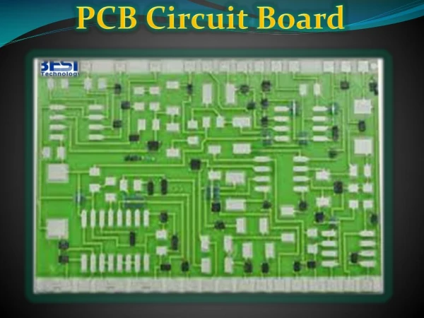
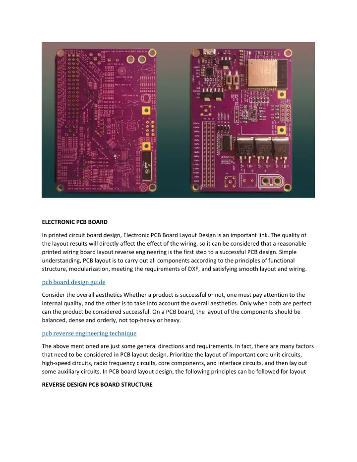
ELECTRONIC PCB BOARD In printed circuit board design, Electronic PCB Board Layout Design is an important link. The quality of the layout results will directly affect the effect of the wiring, so it can be considered that a reasonable printed wiring board layout reverse engineering is the first step to a successful PCB design. Simple understanding, PCB layout is to carry out all components according to the principles of functional structure, modularization, meeting the requirements of DXF, and satisfying smooth layout and wiring. pcb board design guide Consider the overall aesthetics Whether a product is successful or not, one must pay attention to the internal quality, and the other is to take into account the overall aesthetics. Only when both are perfect can the product be considered successful. On a PCB board, the layout of the components should be balanced, dense and orderly, not top-heavy or heavy. pcb reverse engineering technique The above mentioned are just some general directions and requirements. In fact, there are many factors that need to be considered in PCB layout design. Prioritize the layout of important core unit circuits, high-speed circuits, radio frequency circuits, core components, and interface circuits, and then lay out some auxiliary circuits. In PCB board layout design, the following principles can be followed for layout REVERSE DESIGN PCB BOARD STRUCTURE
Reverse Design PCB Board Structure will be able to draws the PCB board spacial structure in the printed circuit board structural designing environment which is a critical part for reverse engineering circuit board, according to the determined circuit board size and various mechanical positioning on the printed circuit card surface, and place the required connectors, buttons/switches, screw holes, assembly holes, etc. printed circuit boards assembly According to the PC Board component positioning requirements. And fully consider and determine the wiring area domain and non-wiring area (such as how much area around the screw hole belongs to the non-wiring area). PCB board manufacturing Reverse Design PCB Board Structure is often the first step for everyone to consider when the schematic diagram is transferred to PCB design. It is also a crucial step in printed circuit board layout redesign. How to build a circuit board copy The quality of the structure of the PCB board is even directly related to the cost of the circuit board manufacturing and the quality of the EMC performance. The following briefly introduces the design of PCB stack structure from two aspects of PCB layer estimation and manufacturability.