Download

1 / 3
30 likes | 42 Views
PCB is a vital element of an electronic circuit design process, and it is essential to know how to design a PCB board assembly.

E N D
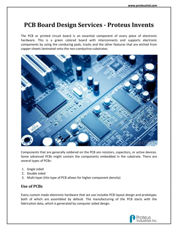
Design Your PCB Board Assembly in an Effective Manner PCB is a vital element of an electronic circuit design process, and it is essential to know how to design a PCB board assembly. The print circuit board layout and design have a significant impact on the way in which a circuit works. As a result, the channel will perform more reliably and within its specification, if the printed circuit board designed efficiently. There are several key stages an individual must understand and know how to commence to produce the best print circuit board design for a given application. As a result of the complexity, there are many CAD, computer aided design packages for commercial development programmes. Long gone are those days where the process of old PCB board assembly design was done by using tape placed on a master drawing sheet. Although, in some limited cases, it is possible that this might still be ingested. Considerably, the capability of print circuit board software varies and into the design, the top end packages enable many more facilities to be incorporated. Whereas, budget or free software provides the necessary functions. Facilities like complex routing, simulations and more are available. With the speeds of digital boards increasing, the ability to undertake simulations is becoming a growing requirement, and the frequency of radio design is reaching even higher. Capture the schematic for the circuit
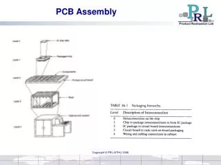
The development of a PCB board assembly design is the circuit schematic capture, which is the first stage and can achieve in many ways. Into a schematic capture tool, the entrance of circuits is entirely possible and can even form a part of the PCB design suite or else be an external package whose output might export in a suitable format. At this stage, the simulations of the circuit may undertake in addition to purely performing the schematic capture, but to simulation packages, few may be able to interface. Without building a prototype, applications such as RF circuit design simulation of the circuitry will enable the final circuit to be optimized more. With the completion of schematic capture, the design of the wiring is contained within the file and can convert to the term "netlist," which is the interconnectivity information. Initial PCB component placement It is essential first to have a rough idea about the sufficient space on the board and where components will be located to contain all the required circuitry, before proceeding with the detailed PCB design and layout. As a result, this will enable decisions about the number of layers needed for the board. A more detailed component layout can be made for the PCB design once a rough estimate of the location and space of the components is complete. As a result, aspects like the proximity of devices which may require to communicate with each other can take into account. Also, additional information about any RF considerations. Therefore it is a must to have all the relevant information associated with PCB board assembly design, so that the components can be incorporated, which includes any drilling information, the footprint for the printed circuit board pads, keep out areas and the like. As the same footprint possibly shared with several devices, the report does is not required to enter for each part. Hence, within the PCB board assembly design and layout system, a library for all the devices used will be built up, where the components used previously can easily be denominated. PCC specializes in rapid PCB assembly and Electronic Manufacturing Services (EMS). We provide the best PCB Assembly Services for low and medium volume, high mix products, to varied customer markets across the global. Right from Design of Manufacturing (DFM), material sourcing, to testing, PCC provide in-house, end to end support services to deliver quick turnkey PCB assemblies and consignments.