Download
1 / 37
420 likes | 824 Views
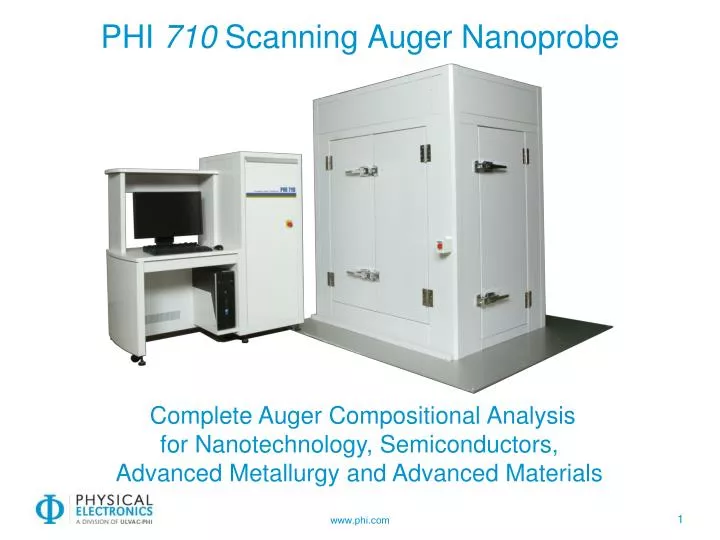
PHI 710 Scanning Auger Nanoprobe. Complete Auger Compositional Analysis for Nanotechnology, Semiconductors, Advanced Metallurgy and Advanced Materials. PHI Auger 710 Superior Analytical Capabilities. Nanoscale image resolution Image registration for high sensitivity

E N D
PHI 710Scanning Auger Nanoprobe Complete Auger Compositional Analysis for Nanotechnology, Semiconductors, Advanced Metallurgy and Advanced Materials
PHI Auger 710Superior Analytical Capabilities • Nanoscale image resolution • Image registration for high sensitivity • Constant sensitivity for all sample geometries • High sensitivity at low tilt angles for insulator analysis • Nano-volume depth profiling • Chemical state analysis: spectra, imaging, depth profiling
PHI 710 Secondary Electron Imaging (SEI)3 nm from Au Islands on Carbon
PHI 710: High Spatial Resolution Auger BAM-L200 Standard Sample 4 nm Al Line AlGaAs Line Width (nm) Area Analyzed Locations for Line Scans 1 2 Auger Line Scans 3 4 Ga Map 25kV; 1nA 256x256 pixels Line Analysis Al Map 25kV; 1nA 256x256 pixels Line Analysis 24 Hour stability test demonstrating exceptional image registry Sample provided by Federal Institute for Materials Research and Testing (BAM) Berlin, Germany
PHI 710: High Spatial Resolution Auger BAM-L200 Standard Sample Line Scan #4 Ga Intensity Al (X3) 4 nm Line 0 0.05 0.1 0.15 0.2 0.25 0.3 0.35 Distance (µm) 24 hour analysis demonstrating exceptional image registration
Constant Sensitivity for All Geometries Sensitivity vs. Sample Tilt Field Emission Electron Source Minimum Beam Diameter 2,000 Multi-Channel Detector 1,800 1,600 1,400 1,200 1,000 Sensitivity (kcps) Coaxial CMA 800 600 Cylindrical Mirror Analyzer 400 Non-Coaxial SCA 200 0 -90 -75 -60 -45 -30 -15 0 15 30 45 60 75 90 Tilt Angle (degree) The CMA with a coaxial electron gun provides high sensitivity at all sample tilt angles which is essential for insulator analysis Ar+ Ion Gun Sample holder with high energy resolution optics
CMA with Coaxial Electron Gun Only the PHI 710can image samples such as FIB sections with uniform, high sensitivity Poly-Si/W Deposition and PatterningAuger Analysis of ex situ FIB cut • Auger maps show: • Defect is sub-micron Si oxide particle • Surrounded by elemental Si • Introduced during poly-Si deposition • Covered with W Auger Maps: Si oxide Si elemental W
PHI CMA High Energy Resolution Mode • How does the high energy resolution mode work? • The CMA energy resolution is given as: • ΔE / E = 0.5% • An optics element placed between the sample surface and the entrance to the standard CMA retards the Auger electrons, reducing their energy, E • From the energy resolution equation, if E is reduced, ΔE is also reduced and so is the Auger peak width; energy resolution is improved • The CMA is not modified in any way and retains a 360º coaxial view of the sample relative to the axis of the electron gun • US Patent 12 / 705,261
PHI CMA High Energy Resolution Mode 710Energy Resolution Specification 0.6 0.5 0.4 ΔE / E (%) 0.3 0.2 0.1 0.0 0 500 1000 1500 2000 2500 Auger Peak Kinetic Energy (eV)
PHI CMA High Energy Resolution Mode Al KLL Spectra of Native Oxide on Al Foil 350 0.5% 0.1% 300 250 200 150 N(E) cps 100 50 0 1393.4 (Al metal) 1386.9 eV (Al oxide) -50 1350 1360 1370 1380 1390 1400 1410 1420 Kinetic Energy (eV) Auger KLL spectrum of native oxide on Al foil measured on PHI CMA at0.5% (blue) and 0.1% (red) energy resolution, after background subtraction.
PHI CMA High Energy Resolution Mode Zn LMM Spectra of Sputter Cleaned Zn Metal 1 0.5% Energy Resolution 0.1% Energy Resolution 0.9 0.8 0.7 0.6 Normalized Intensity 0.5 0.4 0.3 0.2 0.1 0 970 980 990 1000 1010 1020 1030 Kinetic Energy (eV)
PHI CMA High Energy Resolution Mode Depth Profile of Native Oxide on Si 0.1% Energy Resolution 4 x 10 Si elemental 8 6 Si oxide 4 Si plasmons c/s 2 0 10 kV - 10 nA 20 µm defocused beam 4 minutes per cycle -2 60 40 20 1630 1620 1610 0 1600 1590 1580 Kinetic Energy (eV)
PHI CMA High Energy Resolution Mode Depth Profile of Zn Oxide on Zn Zn oxide Zn metal 5 x 10 9.8 9.6 9.4 9.2 c/s 9 10 8.8 5 8.6 8.4 0 970 980 990 1000 1010 1020 1030 Kinetic Energy (eV)
PHI 710 Spectral Window Imaging A B C Si KLL Peak Area SEI Silicide D F E Si Chemical States Si Oxynitride Elemental Si Panel A shows a 200 µm FOV SEI of a semiconductor bond pad. Panel B shows the Si KLL peak area image from the area of panel A. Panels C, D and E show the chemical state images of silicide, elemental Si and Si oxynitride respectively. Panel F shows a color overlay of elemental silicon, silicide and silicon oxynitride images.
PHI 710 Spectral Window Imaging Panel A shows the Si KLL spectrum from the sum of all pixel spectra in the Si KLL Auger image shown in panel B. Panel B shows the three Regions Of Interest (ROI) selected for creation of the basis spectra for Linear Least Squares (LLS) fitting of the Si KLL image data set. Panel C shows the three basis spectra with their corresponding chemical state identifications. A B Composite Si KLL Si KLL image with ROI areas C Intensity Si KLL Basis Spectra PHI App. Note: Chemical State Imaging With The PHI 710 Scanning Auger NanoProbe Si Oxynitride Silicide 1605 1615 1625 Kinetic Energy (eV) Intensity Elemental Si 1604 1608 1612 1616 1620 1624 Kinetic Energy (eV)
Nanocone Imaging SEI N Map 256 x 256 pixels HR Si-oxide Map at 0.1% Energy Resolution Auger Images Suggest Larger Nanocone Surface Composed of Silicon Oxide and Nitride Smaller Silicon Oxide Feature Smaller Silicon Oxide Feature 2O kV – 10 nA Only the larger Nanocone contains N Both the large and small features contain Silicon oxide The composition suggested by the images is confirmed with high energy resolution analysis
Nanocone Chemical Analysis Large Nanocone Base 0.1% Energy Resolution Si Oxide Standard Si Nitride Standard 1 Si KLL 0.8 0.6 Normalized Intensity 0.4 0.2 20 kV – 10 nA 0 1600 1605 1610 1615 1620 1625 1630 Kinetic Energy (eV) Nanocone base is mixture of silicon oxide and silicon nitride
PHI 710Advantages • World’s best Auger depth profiling • Floating column ion gun for high current, low voltage depth profiling • Compucentric Zalar Rotation™ maximizes depth resolution • Image registration maintains field-of-view
Low Voltage Depth Profiling Al Al Intensity Intensity Ga Ga As As 0 10 20 30 0 200 400 600 800 Sputter Time (min) Sputter Time (min) Improved Interface Definition with use of Ultra Low Ion Energies 500 eV Depth Profile 100 eV Depth Profile Improved definition of layers AlAs/GaAs Super Lattice Sample
Nano Depth Profiling 1 60 nm Diameter Si Nanowire Surface Spectrum of Nanowire A 4 x 10 1 Atomic % Si 97.5 SEI P 2.5 0.5 0 P c/s -0.5 O -1 20 kV, 10 nA, 13 nm Beam -1.5 C Si -2 100 200 300 400 500 600 700 800 Kinetic Energy (eV) P from the growth gas is detected on the surface of a Si nanowire
Non-homogeneous P Doping of Si Nanowires Depth Profile of Nanowire B • 500 V Ar sputter depth profiling shows a non-homogeneous radial P distribution. • The data suggests Vapor-Solid incorporation of P rather than Vapor-Liquid-Solid P incorporation
Compucentric Zalar Rotation Depth Profiling Ion Beam CompucentricZalar rotation depth profiling defines the selected analysis point as the center of rotation. This is accomplished by moving the sample in X and Y while rotating, all under software control. Micro-area Zalar depth profiling is possible on features as small as 10 µm with the 710’sautomated sample stage. Analysis Area Sample Zalar rotation is used to eliminate sample roughening that can occur when sputtering at a fixed angle.
Compucentric Zalar Rotation Depth Profiling Compucentric Zalar Depth Profile of 10 µm Via Contact 100 Si Al (metal) 80 O 60 Atomic Concentration (%) 40 Al (oxide) 20 Secondary Electron Image (Before Sputtering) 0 0 50 100 150 200 250 300 Sputter Time (min)
Compucentric Zalar Rotation Depth Profiling Depth Profile Comparison With and Without Zalar Rotation 100 100 Si Si Al (metal) Al (metal) 80 80 O O 60 60 Atomic Concentration (%) Atomic Concentration (%) 40 40 Al (oxide) Al (oxide) 20 20 0 0 0 50 100 150 200 250 300 0 50 100 150 200 250 300 Sputter Time (min) Sputter Time (min) With Rotation Without Rotation
Compucentric Zalar Rotation Depth Profiling SE Images of 10 µm Via Contacts after Depth Profiling 2500X 2500X With Rotation Without Rotation
Large Area Chemical Depth Profile of Ni/Si WaferAnnealed at 425 ºC Elemental Depth Profile 300 0.1% Energy Resolution 10 kV-10 nA 20 µm Average As Received Ni LMM Sputter Conditions: 500 V Argon 1 x 0.5 mm raster No Zalar Rotation 10° Sample Tilt Si KLL 200 Intensity (kcps) 100 Chemical State of Ni ? Chemical State of Si ? 0 0 10 20 30 40 50 60 Sputter Time (min)
Large Area Chemical Depth Profile of Ni/Si WaferAnnealed at 425 ºC Si Chemical Depth Profile Created Using Linear Least Squares Fitting Si KLL 200 Si in Si substrate 100 Intensity (kcps) Si in Ni layer 0 0 10 20 30 40 50 60 Sputter Time (min)
Large Area Chemical Depth Profile of Ni/Si WaferAnnealed at 425 ºC 0.1% Energy Resolution Si basis spectra for LLS (expanded) Si basis spectra for LLS Si KLL Si KLL Si in Si substrate Si in Si substrate Si in Ni layer Si in Ni layer Normalized Intensity Normalized Intensity 1570 1590 1610 1630 1610 1615 1620 1625 Kinetic Energy (eV) Kinetic Energy (eV) 1616.5 eV (metal) 1617.2 eV (silicide)
Large Area Chemical Depth Profile of Ni/Si WaferAnnealed at 425 ºC Si Chemical Depth Profile Created Using Linear Least Squares Fitting 300 0.1% Energy Resolution Ni LMM Ni in Ni layer Ni in Si substrate 200 Intensity (kcps) 100 0 0 10 20 30 40 50 60 Sputter Time (min)
Large Area Chemical Depth Profile of Ni/Si WaferAnnealed at 425 ºC 0.1% Energy Resolution Ni basis spectra for LLS Ni basis spectra for LLS (expanded) Ni LMM Ni LMM Ni in Si substrate Ni in Si substrate Ni in Ni layer Ni in Ni layer Normalized Intensity Normalized Intensity 830 835 840 845 850 855 860 810 820 830 840 850 860 870 880 Kinetic Energy (eV) Kinetic Energy (eV) 844.8 eV (Ni-silicide) 846.2 eV (Ni-metal)
Large Area Chemical Depth Profile of Ni/Si WaferAnnealed at 425 ºC After Depth Profile 2 2.5 Si Si 2.0 Ni Point 1 Ni Ni 1 Ni | Intensity (Mcps) | Si | 1.5 | Point 2 C Si 1.0 C 22 nm beam size SEM 20kV - 1nA Analysis points 500 1000 1500 2000 Kinetic Energy (eV) Point 1: Ni-silicide Point 2: Si-metal • Auger multi-point analysis shows composition of nano-structures
Large Area Chemical Depth Profile of Ni/Si WaferAnnealed at 425 ºC After Depth Profile 0.1% Energy Resolution Si KLL Si KLL (expanded) 22 nm beam size Point 1 Si in Ni layer Point 1 Si in Ni layer Point 2 Si in Si substrate Point 2 Si in Si substrate Normalized Intensity Normalized Intensity 22 nm beam size 1570 1580 1590 1600 1610 1620 1630 1640 1610 1615 1620 1625 Kinetic Energy (eV) Kinetic Energy (eV) 1616.5 eV (metal) 1617.2 eV (silicide)
Ni/Si Annealed at 425 °C 2 1 12 nm Removed Nano-areas selected for depth profiling 2 1 Auger Color Overlay 20 kV - 10 nA 256 x 256 pixels SEM 20 kV - 10 nA Analysis points
Nano Area Chemical Depth Profile of Ni/Si WaferPoint 1 – Ni Layer Chemical Depth Profile Created Using Linear Least Squares Fitting Ni metal Si metal 200 Intensity (kcps) Sputter Conditions: 500 V Argon 1 x 0.5 mm raster No Zalar Rotation 10° Sample Tilt 10 kV – 10 nA Point 1 LLS Profile 100 Ni silicide Si silicide 22 nm beam size 0 0 20 40 60 80 100 120 140 160 180 200 Sputter Depth (nm) • Nano area depth profile shows nickel silicide at the nickel / silicon interface • Large area depth profile included heterogeneous distributions of nickel silicide that grows through imperfections in Ni film
PHI 710Scanning Auger NanoprobeMulti-technique Options Energy Dispersive Spectroscopy (EDS or EDX) Backscatter Electron Detector (BSE) Electron Backscatter Diffraction (EBSD) Focused Ion Beam (FIB) The Complete Auger Solution
PHI 710Scanning Auger Nanoprobe Complete Auger Compositional Analysis for Nanotechnology, Semiconductors, Advanced Metallurgy and Advanced Materials