Download
1 / 49
490 likes | 730 Views
ELECTRON -SPECIMEN INTERACTIONS SPECIMEN PREPARATION ELECTRON MICROSCOPES . EML 5930 (27-750) Advanced Characterization and Microstructural Analysis A. D. Rollett, P.N Kalu Spring 2008. Electron Target Interactions: Electron Optical Imaging and chemical analysis are based upon Detecting ,

E N D
ELECTRON -SPECIMEN INTERACTIONSSPECIMEN PREPARATIONELECTRON MICROSCOPES EML 5930 (27-750) Advanced Characterization and Microstructural Analysis A. D. Rollett, P.N Kalu Spring 2008
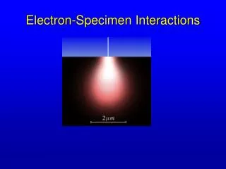
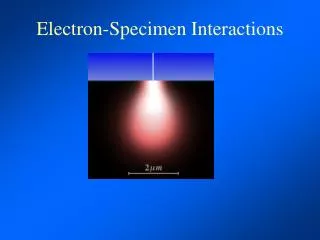
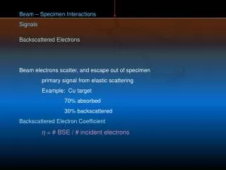
Electron Target Interactions: • Electron Optical Imaging and chemical analysis are based upon • Detecting , • Collecting, and • Processing a range of signals that are produced when an electron beam interacts with either bulk or foil samples. • Figures 9(a) and (b) show beams of high energy electrons interacting with bulk and foil samples respectively.
Figure 9(a). A bulk specimen showing the ‘spread’ of the beam and the activated volume giving rise to (i) backscattered, secondary and Auger electrons (ii) characteristic X-rays and (iii) electron current. Typical values given for the depth of electron penetration and the excited volume for a 30keV, 100nm diameter electron probe.
Figure 9(b). A foil specimen of thickness, t, (t < 300nm) where in addition to (a) transmitted signals give (i) image contrast and electron diffraction and (ii) Kikuchi diffraction
Figure 10 shows the interaction volume as a function of beam energy (Monte Carlo calculations). • The penetration of an electron into a solid depends on the beam energy, which in turn depends on the accelerating voltage, usually between 20 kV and 1,000 kV.
10 kV 20 kV
30 kV Figure 10. Monte Carlo calculations of the interaction volume in iron as a function of beam energy: (a) 10 kV (b) 20 kV, and 30 kV.
SPECIMEN PREPARATION METHODS BULK SAMPLES: Specimens for OPTICAL or SEM examination must be prepared via a sequence of polishing stages, except for: (i) Non conducting specimens – the specimen surface must be coated with gold or carbon. This procedure is not needed if Environmental Scanning Electron Microscope (ESEM) is used. (ii) Fracture Evaluation or Failure Analysis - the specimen must be preserved and the fracture surface should be covered and padded (if possible) for protection against further damage. On no account should the fracture surface be subjected to any form of polishing.
POLISHING STAGES • Mechanical Grinding – This is a form of Rough Polishing, which involves using different grades (or grits) of SiC abrasive papers/belts/cloths, with water as lubricant. A commonly employed grit sequence uses 120-, 240-, 320-400- and 600- mesh abrasive papers. The initial grit size depends on the surface roughness and the depth of damage from sectioning. Sample orientation must be continuously changed to avoid comet tailing.
Mechanical Polishing – After grinding to a 600- grit finish, the sample is polished to produce a flat, reasonably scratch-free surface with high reflectivity. (i) Coarse polishing (30 to 3 m finish) - on special cloths smeared with diamond paste plus some lubricant. (ii) Fine polishing ( 1 m finish) - use diamond paste plus lubricant or Silica or alumina plus water lubricant. (3) Electropolishing or Electrolytic Polishing – This is a process whereby a mechanically polished sample is made smooth and brighter by making the sample the anode in an electrolytic cell. This is only possible when the correct combination of bath temperature, voltage, current density and time is employed.
(4) Chemical Polishing – This procedure can be used instead of (3). It is a method for obtaining a polished surface by immersion in or swabbing with suitable solution without need of an external electric current. NOTE Specimens for Electron Backscattered Diffraction (EBSD) analysis or Orientation Imaging Microscopy (OIM) may require special specimen preparation methods. This will be discussed latter.
SPECIMENS FOR TEM • Specimens are usually in one or two forms: • Replica • Thin foil REPLICAS: • These are prepared by different techniques: • Surface or Carbon replica • “Extraction” replica
SURFACE or CARBON REPLICA: • This is produced from a specimen as prepared for light microscopy i) The specimen surface is coated with a cellulose acetate film (e.g., collodion) to produce a negative impression of the surface features. ii) The plastic film is stripped from the specimen surface and coated with a layer of carbon (about 10 to 20 nm thick). The carbon-coating process takes place in a vacuum evaporator unit. iii) The plastic is then removed (dissolved) from the carbon replica by solvent. iv) Before the replica is observed in the microscope, it is usually shadowed (sputtered) with carbon or a heavy element to enhance the topographical features of the surface.
“EXTRACTION” REPLICA: i) The metallographic specimen is etched beforehand to put particles and carbides in relief. ii) Carbon film is deposited on the surface of the etched specimen. iii) The carbon film itself is not physically stripped from the specimen surface, but etched or “floated” away from the surface so that those particles attached to the deposited carbon film will be extracted from the specimen. THIN FOIL PREPARATION: • Electropolishing: window technique disk method jet thinning • Ion Beam Thinning • Chemical Polishing
window technique Figure 11. Typical stages in electropolishing sheet material using the window technique. The shaded regions a-d are lacquered.
disk method Figure 12. (a) Anode current density I vs. specimen potential E. Curve ABCD shows a polishing plateau BC whereas curve EF does not. (b) Schematic diagram illustrating potentiostatically controlled electropolishing
Jet thinning Figure 13. Schematic diagram illustrating the action of an a.c. jet thinning technique due to Bainbridge and Thorne.
Ion Beam Thinning Figure 14. Schematic diagram of typical ion-beam thinning equipment
Figure 15. Schematic diagrams showing (a) the depth of penetration of argon ions as a function of the angle between the beam and specimen, and (b) the variation of thinning rate with angle of beam incidence
Other Thin-Foil Preparation Techniques • Microtomy Replicas • Single-stage replicas 1. Deposit carbon (100-200A) on surface of interest 2. Remove by etching the specimen to free the porous film and “floating’ the film off the specimen 3. Shadow with a heavy element (gold or silver) • Two-stage replicas • Extraction replicas - useful for small particle ID and characterization
Artifacts in Thin Foils • Careless Handling: Dislocations, Bend Contours, Cracks • Careless Washing: Surface films/deposits • Hydrogen Contamination: During electropolishing with acid electrolytes (Ti and Zr alloys) • Interstitial Contamination during electropolishing or storage (Nb and Ta) • Surface Oxidation even during examination in the microscope- can effect structure (stacking faults, extra reflections of Moire patterns if the oxide is crystalline) or apparent composition; also, surface mottling common; streaks in diffraction pattern
Artefacts in Thin Foils Continued • Electron or ion beam damage in the microscope--may produce dislocation loops • Ion Beam damage during ion beam thinning • Heating during ion beam thinning or examination might cause microstructural changes, e.g., crystallization • Uneven polishing--surface etching or mottling; redeposition of precipitates on the surface of the foil • Dislocations might move and/or annihilate when a thin foil is produced--especially in materials with low lattice resistance (Peierl’s stress); Likewise, dislocations might dissociate to form visible stacking faults due to local stresses-- not representative of bulk behavior
Artefacts in Thin Foils Continued • Martensite or other displacive transformations might form spontaneously in thin regions of the foil even above Ms (Ti, Zr, and Fe alloys) • Deformation twinning might occur in bent foils but not in the bulk • Hot stage work might result in precipitates nucleating on the surface (not representative of the bulk) • Metastable b.c.c. Ti alloys can transform via twinning to produce planar features
The Instrument- • SEM is primarily used to study the surface, or near surface structure of bulk specimens. • The electron gun, condenser lenses and vacuum system, are similar in SEM and TEM. • A schematic diagram of the electron optical column for a two lens scanning electron microscope (SEM), is presented in Figure 16.
Figure 16. Schematic diagram of a scanning electron microscope.
The electron gun produces electrons, and accelerates them at the operating voltage. • The operating voltage ranges from 0 to 30 – 60 kV depending upon the type of instrument. • Figure 17 shows a typical configuration of an electron gun.
The microscope is a probe forming system. • Two or three condenser lenses demagnify the electron beam until it hits the specimen surface as a focused spot or probe. • Electron probes of sizes down to ~ 6 nm are attainable with conventional thermionic emission sources, although smaller probes ~ 2 nm can be achieved using field emission sources.
The fine beam of electrons is scanned across the specimen by deflector coils. • The low energy electrons or other radiation emitted from the surface are detected/collected and amplified to form a video signal, which modulates the brightness of a cathode-ray tube (c.r.t.) display. • The electron beam and the c.r.t. spot are both scanned in a similar way to a television receiver, that is in a rectangular set of straight lines known as raster.
Imaging Modes and Information- • The different signals produced when the electron beam interacts with the bulk sample in the SEM are used to create an image. • One of the main features of the SEM is that, in principle, any radiation emitted from the specimen or any measurable change in the specimen can be used to provide the signal to modulate the c.r.t., and thus provide the contrast. • The various methods used to collect these emitted electron signals are summarized in Figure 18.
Figure 18. Methods of detecting electrons in a scanning electron microscope (a) secondary electrons (b) backscattered electrons, solid state detector (c) backscattered electrons, scintillation counter, and (d) absorbed electron current.
Table 3. Commonly Used Scanning Electron Microscopy Imaging Modes Together with Resolution Attainable
(a) Topographic Images: • One of the principal uses of SEM is to study the surface features, or topography of a sample. • Although this form of image may be obtained using most signals, secondary or backscattered electrons are usually recommended.
Secondary Electrons • Secondary electrons are detected by a scintillator - photomultiplier system known as the Everhart-Thorny detector • The number of detected secondary electrons increase with surface tilt. About 20 to 40 degrees specimen tilt towards the detector may be necessary. • Topographic images obtained with secondary electrons look remarkably like images of solid objects viewed with light. • We find these topographic images easy to interpret.
Backscattered Electrons • Topographical images may be obtained by using Backscattered electrons, which are detected with: (i) scintillator - light pipe - photomultiplier (e.g. Robinson detector) type detectors, known for their rapid response time, or (ii) solid state detectors, with a disadvantage of relatively slow response time.
(b) Compositional Images: • Backscattered electrons and X-rays from the specimen is also capable of yielding composition information. Backscattered Electrons • The composition of samples are sensitive to backscattered coefficient (), which varies monotonically with atomic number. • It has been shown that the coefficient can be expressed as: 13
The magnitude of the compositional or atomic number contrast from two phases of backscattered coefficients 1 and 2 is readily calculated as: 14 • This method is not recommended for phases with similar atomic number, as the resolution may be very poor.
Quantitative compositional information for phases of low atomic number can be obtained by comparing the intensity of the backscattered signal from the phases with a standard element. Care must be taken. • Such information is not easily determined using X-ray method.
X-ray Microanalysis • The characteristic X-rays emitted by bombarding specimen with high-energy electrons may be identified from either wavelength or characteristic energy since: where h is the Planck’s constant and c is the velocity of light. • Equation (15) forms the basis of techniques which use characteristic X-rays for compositional analysis. • There may be other spectroscopic and microanalytical techniques, X-ray microanalysis is excellent for routine chemical analysis of small volumes (15)
The analytical techniques rely on the efficient detection and discrimination of X-rays. • Detection of the X-rays can be accomplished by using any of the following methods: • Energy Dispersive Spectroscopy (EDS) • on scanning and transmission electron microscopes • Wavelength Dispersive Spectroscopy (WDS) • on electron microprobes • Electron Energy Loss Spectroscopy (EELS)
Figure 19(a). Wavelength dispersive crystal spectrometer: Collection of X-rays by spectrometer; generated X-rays have a range of wavelengths, Dl, but only one is selectively diffracted to the detector.
Figure 19(b). The constant take off angle and change of crystal position required to retain focussed condition.
Table 4. Crystals Used in Wavelength Dispersive Spectrometers
Figure 20. Gas-flow, argon/methane or xenon, proportional counter used in conjunction with a crystal spectrometer.
Figure 21. X-rays enter energy dispersive spectrometer through a thin Be window and produce electron-hole pairs within the semiconductor crystal. A typical energy spectrum obtained from a general area of a ferric stainless steel is shown.
(c) Crystallographic Information: • There are three SEM-based techniques for obtaining crystallographic information from samples. These are: • Kossel technique • Electron Channeling Diffraction, and • Electron Backscattered Diffraction technique
Figure 22. Electron channel pattern: The production of channel patterns
Figure 23 : Electron channel pattern obtained from a gallium phosphide crystal of (111) of orientation.