Download
1 / 10
100 likes | 182 Views
HCAL DAQ E. Garutti, M. Groll and a lot of help from Paul and Matthias. Present Status. Hardware: 64X VME crate installed SBS driver installed / functional Use ECAL prototype CERC board DAQ: communication to VME established

E N D
HCAL DAQE. Garutti, M. Grolland a lot of help from Paul and Matthias
Present Status Hardware: • 64X VME crate installed • SBS driver installed / functional • Use ECAL prototype CERC board DAQ: • communication to VME established • detailed HCAL software required for shift register handling being written NOW • test of FE electronics soon to come
The VME crate Multiplexed ASICs Piggy backs on L/R HAB VME FE connections 7608 SiPM / (18 * 6 * 2 * 8) = 5 CRC needed for r/o (38 cables) use left and right connectors to VME for L/R HBAB 424 PIN diode / (18 * 6 * 2 * 8) = 2 cables Total of 5 CRC L/R connectors
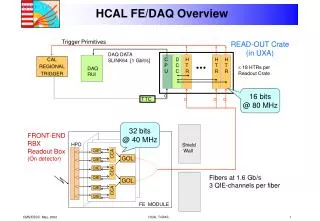
The Readout Board Readout board structure • Front End (FE) FPGA controls all signals on VFE-PCB cable • Back End (BE) FPGA gathers and buffers all event data from FE and provides interface to VME 40 MHz clock 25ns timing possible • Trigger logic in BE for timing and backplane distribution; only active in one board FE BE
Readout board features • Sample-and-hold timing needs to be better than 10ns • Fine-tune rising edge of signal on 4 clock, ~6.25 ns steps • Each FE cable can be timed independently • Dual 16-bit ADCs and 16-bit DAC • DAC fed back for internal as well as VFE calibration • No data reduction planned in hardware • Read out all channels for every event • 2 Bytes 1728 channels/board = 3.5 kBytes/board • 2 Bytes 8000 channels = 16 kBytes total • On-board 8 Mbytes buffer memory • Allows up to ~500 events for HCAL during beam spill • 1 train = 0.4 s, 1kHz particles 400 particles/train (?)
SR settings Testbeam: 60 s / 20 spills = 3.0 s / spill SR operates with 1kHz 16 bit for switches + 18 x 8 bits for DAC settings 160 bits x 6 HABs 960 bits for each HBAB → 1kHz clock x 960 bits (x 2) = 1-2 s But maybe faster~10kHz Minimum SR changes needed to toggle between physics & calibration mode: 4 bits for shaping time+ 4 bits for gain settings+ 1 bit for injection resistor 9 bits → 0,02 s
960bits 2ms 1 s 10ms 70ms Event readout Define operating parameters SW_DAC_IN: disconnect ASIC from SIPM during programmingLED_SEL: toggle TCALIB to CMB (LED) or to ASIC (charge injection)VCALIB: amount of charge or LED amplitude
Event Timing • Shift Register:operates with 1kHz or 10kHz clock→ 1/1000 s x 960 bits (x 2 HBAB) ~ 0.1-1 s→ to switch between calibration and physics mode and back: ~5-8 s • DAQ Readout: timed in units of 25 ns (40MHz clock)VFE clock start: 10 ms after verification bit (?) VFE Multiplex clock: 18ch x 4 ms (1 clock cycle) = 72 msHold duration: 50400 x 6.25 ns = 315 msADC start: 7.5 msADC stop: 13500 x 25ns = 337.5 ms→ duration: 330 ms limit 3kHz → maybe possible to reduce since 16-bit ADC r/o at 500 kHz needs only 70 ms for 18ch. • Buffer data to BE 8 MB QDR during the spill, 4byte@160MHz=6ms • transfer from QDR to VME-Bus at equal speed of 6mus. • Read data from VME, 20-30MB/s rate ~400Hz
Readout Timing ← sending settings for SR Measured 140ms/HAB → r/o configuration info + data VFE <-> FE board FE board -> BE board (buffer) 16-bit ADC clocked with 4 ms clock cycles 14 kHz for 18 ch. Presently limited to 3 kHz for safety BE board (buffer) -> VME Transfer time is not a limiting factor ~6mus @ 8MB/s for 0.5k events/FE VME -> PC (HDD -> dCache) Transfer rate ~400Hz Disk write speed: ~ 20 MB/s