Download
1 / 36
380 likes | 575 Views
Scanning Probe Microscopes. Y. Tzeng Auburn University July 2003. (Presented by Tan Zhang for ELEC 7970 instructed by Y. Tzeng, 2003). SPM Family. Scanning Tunneling Microscope - STM Atomic Force Microscope - AFM Force-Modulated AFM (FMM) Lateral Force Microscope - LFM

E N D
Scanning Probe Microscopes Y. Tzeng Auburn University July 2003 (Presented by Tan Zhang for ELEC 7970 instructed by Y. Tzeng, 2003)
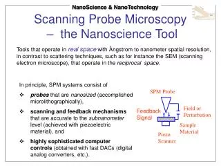
SPM Family Scanning Tunneling Microscope - STM Atomic Force Microscope - AFM Force-Modulated AFM (FMM) Lateral Force Microscope - LFM Magnetic Force Microscope - MFM Scanning Thermal Microscope - SThM Electrical Force Microscope – EFM Near-field Scanning Optical Microscope – NSOM (SNOM) . . . A Whole Family Gerd Binnig and Heinrich Rohrer http://invsee.asu.edu/Invsee/listmod.htm
SPM http://invsee.asu.edu/Invsee/listmod.htm
SPM Tips 4.167 mm 550 nm http://invsee.asu.edu/Invsee/listmod.htm
STM http://invsee.asu.edu/Invsee/listmod.htm
STM/SEM • 6 translational modes of motion; • Independent sample and STM-tip positioning; • Heating and cooling; • Temperature ranging from 60K to 1000K http://www.omicron.de/products/stm_stage/
SEM-assisted STM-tip Approach http://www.omicron.de/products/mslab/uhvlab.html
LT STM Three domains of charge density waves on NbSe2 at T = 5 K in UHV, 5 nm x 5 nm, U(gap) = 0.02 V, I(t) = 2.55 nA). http://www.omicron.de/products/lt_stm/r_ltstm2.html
AFM http://invsee.asu.edu/Invsee/listmod.htm
AFM http://invsee.asu.edu/Invsee/listmod.htm
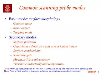
AFM mode Contact mode tips makes contact with the sample; can be performed within a liquid environment; Non-contact mode cantilever vibrates near the surface of the sample; spacing is tens to hundreds of angstroms; Intermittent mode cantilever tips just barely hit or tap the sample; both liquid and air environment; for soft samples.
175 um 2500 um 20 um 9.38 um AFM Tips http://invsee.asu.edu/Invsee/listmod.htm
AFM/STM Contact and non-contact AFM, and STM; Lateral (friction) force detection; Electrostatic, magnetic force imaging; Simultaneous AFM and STM detection http://www.omicron-instruments.com/products/afm_stm/
AFM SEM AFM http://invsee.asu.edu/nmodules/spmmod/timetable.html
AFM A soft polymer material. Density of peptides: a) 1%; b) 10%; c) 100% Field of view: 4.85 µm x 4.85 µm. http://www.pacificnanotech.com/apps/app8.htm
Image of 14 nm diameter colloidal gold spheres. Image range is 4 µm X 4 µm. Image of 28 nm colloidal gold spheres. Image range is 4 µm X 4 µm. AFM-metrology http://www.pacificnanotech.com/apps/app8.htm
LFM http://www.ntmdt.ru/applicationnotes/LFM/
LFM Bi-Cell PSPD Quad-Cell PSPD http://invsee.asu.edu/Invsee/listmod.htm
LFM and PCM Topography (left) and Lateral Force images (right) of a structured polymer material. Topography, right, and Phase Contrast, left, images of a co-block polymer. PCM – Phase Contrast Mode http://www.pacificnanotech.com/apps/app8.htm
FMM http://invsee.asu.edu/Invsee/listmod.htm
FMM Topographic contact AFM image (left) and FMM image (right) of CF/polymer composite. http://invsee.asu.edu/Invsee/listmod.htm
MFM http://invsee.asu.edu/Invsee/listmod.htm
MFM Magnetic switching of nanostructured cobalt islands http://www.ee.umd.edu/~rdgomez/cobalt_animation.htm
MFM -- Domain Wall Motion of Small Permalloy Elements http://www.ee.umd.edu/~rdgomez/Permalloy.htm
NSOM http://www.triple-o.de/pages/application_spm.html#snom
NSOM The SNOM sensor enables convenient, non-destructive imaging of premounted IC structures. http://www.snom.omicron.de/examples/twinsnom/x-tsnom_6.html
TwinNSOM http://www.snom.omicron.de/instruments/twinsnom/tech.html
http://www.nanotechnologyinstitute.org/presentations/IMECE01_NANO1_Li_2.pdfhttp://www.nanotechnologyinstitute.org/presentations/IMECE01_NANO1_Li_2.pdf
http://www.nanotechnologyinstitute.org/presentations/IMECE01_NANO1_Li_2.pdfhttp://www.nanotechnologyinstitute.org/presentations/IMECE01_NANO1_Li_2.pdf
Fabrication of thermal microprobes with a sub-100 nm metal to metal junction INSTITUTE OF PHYSICS PUBLISHING Nanotechnology 13 (2002) 29–32 D W Lee1,4, Takahito Ono2 and Masayoshi Esashi3 http://www.nanotechnologyinstitute.org/presentations/IMECE01_NANO1_Li_2.pdf
http://www.nanotechnologyinstitute.org/presentations/IMECE01_NANO1_Li_2.pdfhttp://www.nanotechnologyinstitute.org/presentations/IMECE01_NANO1_Li_2.pdf
http://www.nanotechnologyinstitute.org/presentations/IMECE01_NANO1_Li_2.pdfhttp://www.nanotechnologyinstitute.org/presentations/IMECE01_NANO1_Li_2.pdf
http://www.nanotechnologyinstitute.org/presentations/IMECE01_NANO1_Li_2.pdfhttp://www.nanotechnologyinstitute.org/presentations/IMECE01_NANO1_Li_2.pdf http://arjournals.annualreviews.org/doi/full/10.1146/annurev.matsci.29.1.505;jsessionid=igdg5icQTWH9