Download
1 / 18
180 likes | 245 Views
NanoScience & NanoTechnology. Scanning Probe Microscopy – the Nanoscience Tool.

E N D
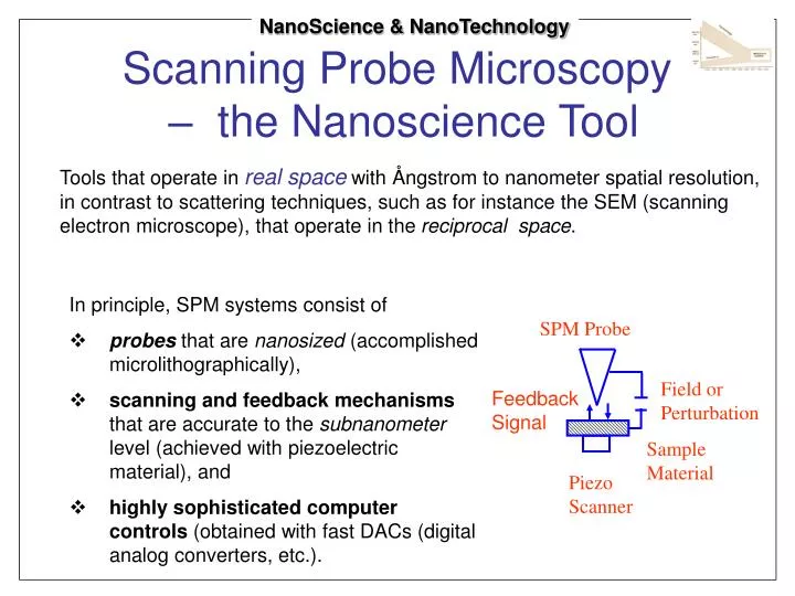
NanoScience & NanoTechnology Scanning Probe Microscopy – the Nanoscience Tool Tools that operate in real spacewith Ångstrom to nanometer spatial resolution, in contrast to scattering techniques, such as for instance the SEM (scanning electron microscope), that operate in the reciprocal space. In principle, SPM systems consist of • probes that are nanosized (accomplished microlithographically), • scanning and feedback mechanisms that are accurate to the subnanometer level (achieved with piezoelectric material), and • highly sophisticated computer controls (obtained with fast DACs (digital analog converters, etc.). SPM Probe Field or Perturbation Feedback Signal Sample Material Piezo Scanner
NanoScience & NanoTechnology SPM - Tree
NanoScience & NanoTechnology SPM – Basic Principles Scanning Tunneling Microscope (STM) Scanning Force Microscope (SFM) Scanning NearField Microsopye (SNOM)
NanoScience & NanoTechnology STM Background In 1981, G. Binnig, H. Rohrer, Ch. Gerber and J. Weibel observed vacuum tunneling of electrons between a sharp tip and a platinum surface. The tunnel current is strongly distance, Dz, dependent; i.e., A=4p(2m)1/2/h, with the tip-sample applied bias voltage, Vbias, and the average potential barrier height F. Tunneling occurs in the low bias voltage regime, i.e., ~0.1 V. At high bias voltage, i.e., Vbias>F/e, the current flow is due to field emission (FE), i.e., (Fowler Nordheim Eq.)
NanoScience & NanoTechnology STM Modes of Operation • Constant height imaging or variable current mode (fast scan mode).The scan frequency is fast compared to the feedback response, which keeps the tip in an average (constant) distance from the sample surface. Scanning is possible in real-time video rates that allow, for instance, the study of surface diffusion processes. • Differential tunneling microscopy Tip is vibrated parallel to the surface, and the modulated current signal is recorded with lock-in technology. • Tracking tunneling microscopy Scanning direction is guided by modulated current signal (e.g., steepest slope). • Scanning noise microscopy Use current noise as feedback signal at zero bias. • Nonlinear alternating-current tunneling microscopy Conventionally, STM is restricted to non-conducting surfaces. A high frequency AC driving force causes a small number of electrons to tunnel onto and off the surface that can be measured during alternative half-cycles (third harmonics).
LASER Photodiode Glass Transition Topography PIEZO AFM Friction Tg = 374K CANTILEVER A B SAMPLE Elasticity Material Distinction NanoScience Tool Scanning Force Microscopy (SFM)
NanoScience Tool SFM Environment Environmental chamber and heating /cooling stage for scanning probe microscope.
NanoScience Tool SFM Modes of Operation Modes of Operation: Provide: • Lateral Force Microscopy • Scanning Modulation Microscopy • Force Approach Spectroscopy • Contact Thermal Shear Modulation Analysis - Imaging (Material Distinction) - Rheological Analysis - Imaging (Material Distinction) - Rheological Analysis - Interaction Forces - Material Compliances - Rheological Boundary Layer - Thermally-Induced Transitions (e.g., glass transition)
SFM Modes of Operation Dx Scan Hysteresis Air or Liquid Environment kL F Lateral Force: FL = kL*Dx 0 SFM Tip x Solid Interface x scan directions Fstatic Fdynamic Topography/Friction Molecular Resolution Molecular Stick Slip Lateral Force Microscopy Material Distinction Rheological Analysis Lateral Force Rate and Thermal Analysis FL Piezo Scanner/ Feedback
SFM Modes of Operation PS 2.2 zresp 2 xresp Tg 95 oC 1.8 1.6 Shear Response 1.4 1.2 1 Modulus and Contact Information x or z modulated piezo 0.8 Si 0.6 50.0 60.0 70.0 80.0 90.0 100.0 110.0 120.0 Temperature (oC) Viscosity and Contact Information Scanning Modulation Microscopy Measured with two-phase lock-in technique Compares response signal to input signal • at constant applied load • with modulation frequencies exceeding feedback response Shear Response and Thermal Analysis Topography Friction "Elasticity" 24oC 94oC 109oC Molecular Resolution
SFM Modes of Operation xresp F xresp(D) F(D) 0 0 D 0 Rheological Boundary Regime xresp Rheological Boundary Regime Probing Distance (D) linearly ramped z-Piezo x-modulation input Force Approach Spectroscopy PS grafted Silicon in (a) water (poor solvent) (b) toluene (good solvent) F(D) Normal Force Response R.M. Overney et al., Phys. Rev. Lett. 76, 1272-1275 (1996).
Entropic Structuring of Simple Liquids Principle Water no boundary layer OMCTS “monolayer" n-C16H34 ~ 3 layers OMCS measurements are in agreement with x-ray reflectivity results (S. Sinha): M. He et al., Phys. Rev. Lett. 88 p.154302/1-4 (2002). X - ray study: H. Kim et al., in Dynamics in Small Confining Systems V, edited by J.M. Drake et al., (Mat. Res. Soc. Symp. Proc. 2001) Vol 651, p T2.1
SFM Modes of Operation Cantilever Tip 127 107 87 d FILM THICKNESS, ( nm ) D x Tg ( OC ) 67 mod 0 50 100 150 200 250 300 105 47 12.0 kDa PS FOX-FLORY (BULK) 27 100 7 104 107 103 105 106 C ) MOLECULAR WEIGHT [Mn] o 95 ( g T 90 85 Contact Thermal Shear Modulation Analysis Shear Response , F D x L Shear Displacement Sample Heating/Cooling Stage C. Buenviaje, et al., ACS symposium series; 781 (2001): 76-92 DxL, F 0 Tg 250 350 360 370 380 400
NanoScience Tool SFM: Other Modes of Operation • Electrostatic Force Microscopy (EFM) Application:Study of the location and lifetime of surface charges on insulating surfaces. Procedure: Long-range electrostatic Coulombic forces are measured with a mechanically modulated conductive or clean silicon cantilever tip. An AC voltage is applied between the tip and the sample with a frequency w2 that is smaller than the mechanical modulation frequency w1 but larger than the gain of the feedback response. The AC voltage causes a charge and a mirror charge on the tip and the sample, respectively. The mechanically modulating tip is experiencing a Coulombic force gradient. For an uncharged surface the force gradient will oscillate at 2w2, whereas for a charged surface, the force gradient will be modulated at w2. A charge signal can be extracted by measuring the f and 2f signal with lock-in technique. The phase of that signal corresponds to the sign of the surface charge. • Magnetic Force Microscopy (MFM) Application: Measuring of surface magnetic structures Procedure: Using the non-contact mode with magnetically coated cantilever tips.
C AFM/SFM Environment Environmental chamber and heating /cooling stage for scanning probe microscope (SFM).
FORWARD Molecular Resolution Lateral Force Image (left) with Molecular Stick Slip behavior (below) Lateral force images on smooth surfaces may be used to distinguished materials displaying different coefficients of friction. REVERSE PHOTODIODE Dx CANTILEVER WITH LATERAL SPRING CONSTANT KL REFLECTED LASER BEAM REVERSE SCAN FORWARD SCAN SAMPLE F FORWARD FL x 0 REVERSE Fstatic Fdynamic SFM Modes Friction Force Microscopy
SFM Modes xresp F xresp(D) F(D) 0 0 D 0 Rheological Boundary Regime xresp Rheological Boundary Regime Probing Distance (D) linearly ramped z-Piezo x-modulation input Force Approach Spectroscopy PS grafted Silicon in (a) water (poor solvent) (b) toluene (good solvent) F(D) Normal Force Response D R.M. Overney et al., Phys. Rev. Lett. 76, 1272-1275 (1996).
SFM/AFM on bilayer Lipid Film Fave=24 nN Tomlinson Model Molecular Stick-Slip Model (1920) R. M. Overney et al., Phys. Rev. Lett. 72, 3546 (1994) NanoScience & Lubrication Molecular Stick-Slip Fave=32 nN