Download
1 / 23
230 likes | 378 Views
EENG 2920: Circuit Design and Analysis Using PSpice Class 3: DC and Transient Analysis. Oluwayomi Adamo Department of Electrical Engineering College of Engineering, University of North Texas. Modeling of Elements. PSpice simulation of circuits is based on the models of circuit elements.

E N D
EENG 2920: Circuit Design and Analysis Using PSpiceClass 3: DC and Transient Analysis Oluwayomi Adamo Department of Electrical Engineering College of Engineering, University of North Texas
Modeling of Elements • PSpice simulation of circuits is based on the models of circuit elements. • A model that specifies a set of parameters for an element is specified in PSpice by the “.MODEL” command. • The general form of the model statement is.MODEL MNAME TYPE (P1=A1 P2=A2 …)TYPE is the type name of the elements and must have the correct model type name (shown in Table 3.2, page 43) • There can be more than one model of the same type in a circuit with different model names. EENG 2920, Class 3
Resistor Models • The name of a resistor must start with R. • Models in PSpice Capture • The user can assign the model name of the breakout devices in the library “breakout.olb” • The user can edit the model parameters. • Model Parameters for Resistors (Table 3.1, page 41) • R: Resistance, no unit, default: 1. • TC1: linear temperature coefficient, unit: oC-1, default: 0. • TC2: quadratic temperature coefficient, unit: oC-2, default: 0. • TCE Exponential temperature coefficient, unit: oC-1, default: 0. • Resistance as a function of temperature: • T and T0 are the operating temperature and the room temperature, respectively, in degree Centigrade EENG 2920, Class 3
A Simple Demo of PSpice Model Editor • This step-by-step demo will show how to do the following: • Add library breakout.olb • Place breakout elements, e.g., Rbreak • Invoke PSpice Model Editor • Create new resistor models • Label breakout resistor models • Run simulations • Show voltages and currents • Edit model parameters • Also demonstrate how to edit property Note: In the Capture CIS that we are using in labs, we have to write “R=.9”, instead of “R=0.90”; that is, you have to remove 0 at both ends. The Lite version does not have such bugs. EENG 2920, Class 3
Example 3.2 • Create a new blank Analog or Mixed A/D project E3_2 • Draw the following circuit: • Resistors are from the library “breakout.olb”, Rbreak • Select one of the Rbreak resistor, right-click mouse, select “Edit PSpice Model” • Create resistor models Rmod1 and Rmod2, save the models: • Correctly label the breakout resistor models: EENG 2920, Class 3
Figure 3.2.1: • Create simulation profile “sim1” • Analysis type is “Bias Point” • Run simulation, show the following simulation results • Try the following menu commands • PSpice – Bias Points • PSpice – Create Netlist, and PSpice – View Netlist EENG 2920, Class 3
Example 3.3 • Create a new blank Analog or Mixed A/D project E3_2 • Draw the following circuit: • Define node numbers: 1, 2, 3, 4. • Create a new simulation profile sim1 • Analysis type is Bias Point • Define parameters to Calculate Small Signal DC Gain (.TF) as shown in the figure: Vin V(2,4) EENG 2920, Class 3
Figure 3.3.1: • Run simulation and obtain the following simulation results: • Check Output File for the Small Signal Characteristics • Go to menu PSpice – View Output File: Figure 3.3.2: EENG 2920, Class 3
Transient Analysis • A transient analysis deals with the behavior of an electric circuit as a function of time. • If a circuit contains an energy storage elements, a transient can also occur in a DC circuit after a sudden change due to switches opening and closing. • PSpice allows simulating transient behaviors, by assigning initial conditions to circuit elements, generating sources, and the opening and closing of switches. • The simulation of transients in circuits with linear elements requires modeling of • Resistors, capacitors, and inductors, • Model parameters of elements, • Operating temperature, • Transient sources. EENG 2920, Class 3
Capacitor • The symbol for a capacitor is C. The name of a capacitor must start with C, and the general form is: • C<name> N+ N- CNAME CVALUE IC=V0where IC is the initial condition, i.e., the initial voltage of the capacitor. • Model parameters for capacitors (Table 4.1, page 86) • C: capacitance multiplier, no unit, default: 1. • VC1: linear voltage coefficient, unit: V-1, default: 0. • VC2: quadratic voltage coefficient, unit: V-2, default: 0. • TC1: linear temperature coefficient, unit: oC-1, default: 0. • TC2: quadratic temperature coefficient, unit: oC-2, default: 0. • Capacitance as a function of voltage and temperature: • T and T0 are the operating temperature and the room temperature, respectively, in degree Centigrade • The capacitor device from “breakout.olb” can be edited and new models can be defined in the same way as resistor. For example, • .MODEL Cmod1 CAP (C=1 VC1=0.01 VC2=0.002 TC1=0.02 TC2=0.005) EENG 2920, Class 3
Inductor • The symbol for an inductor is L. The name of an inductor must start with L, and the general form is: • L<name> N+ N- LNAME LVALUE IC=I0where IC is the initial condition, i.e., the initial current of the inductor. • Model parameters for inductors (Table 4.2, page 88) • L: inductance multiplier, no unit, default: 1. • IL1: linear current coefficient, unit: A-1, default: 0. • IL2: quadratic current coefficient, unit: A-2, default: 0. • TC1: linear temperature coefficient, unit: oC-1, default: 0. • TC2: quadratic temperature coefficient, unit: oC-2, default: 0. • Inductance as a function of voltage and temperature: • T and T0 are the operating temperature and the room temperature, respectively, in degree Centigrade • The inductor device from “breakout.olb” can be edited and new models can be defined in the same way as resistor and capacitor. For example, • .MODEL Lmod1 IND (L=1 IL1=0.1 IL2=0.002 TC1=0.02 TC2=0.005) EENG 2920, Class 3
Exponential Source • The symbol of exponential sources is EXP, and the general form is • EXP (V1 V2 TRD TRC TFD TFC) • Model parameters (Table 4.3, page 91) • V1: initial voltage, unit: V, default: none • V2: pulsed voltage, unit: V, default: none • TRD: rise delay time, unit: S, default: 0 • TRC: rise-time constant, unit: S, default: TSTEP • TFD: fall delay time, unit: S, default: TRD+TSTEP • TFC: fall-time constant, unit: S, default: TSTEP • Among the parameters, V1 and V2 must be specified by the user. EENG 2920, Class 3
Pulse Source • The symbol of pulse sources is PULSE, and the general form is • PULSE (V1 V2 TD TR TF PW PER) • Model parameters (Table 4.4, page 92) • V1: initial voltage, unit: V, default: none • V2: pulsed voltage, unit: V, default: none • TD: delay time, unit: S, default: 0 • TR: rise time, unit: S, default: TSTEP • TF: fall time, unit: S, default: TSTEP • PW: pulse width, unit: S, default: TSTOP • PER: period, second, default: TSTOP • Among the parameters, V1 and V2 must be specified by the user. TSTEP and TSTOP are the incrementing time and stop time, respectively, during the transient analysis. EENG 2920, Class 3
Piecewise Linear Source • The symbol of piecewise linear sources is PWL, and the general form is • PWL (T1 V2 T2 V2 … TN VN) • A point in a waveform can be described by (Ti, Vi) or (Ti, Ii) and every pair of values specifies the source value at time Ti. The voltage at time between the intermediate points is determined by PSpice using linear interpolation. • Model parameters (Table 4.5, page 94) • Ti: time at a point, unit: second, default: none • Vi: voltage at a point, unit: V, default: none EENG 2920, Class 3
Single-Frequency Frequency Modulation • The symbol for a source with single frequency modulation is SFFM, and the general form is • SFFM (VO VA FC MOD FS) • Model parameters (Table 4.6, page 95) • VO: offset voltage, unit: V, default: none • VA: amplitude of voltage, unit: V, default: none • FC: carrier frequency, unit: Hz, default: 1/TSTOP • MOD: modulation index, unit: none, default: 0 • FS: signal frequency, unit: Hz, default: 1/TSTOP • Among the parameters, VO and VA must be specified by user and can be either voltages or currents. EENG 2920, Class 3
Sinusoidal Source • The symbol for sinusoidal source is SIN, and the general form is • SIN (VO VA FREQ TD ALP THETA) • Model parameters (Table 4.7, page 96) • VO: offset voltage, unit: V, default: none • VA: peak voltage, unit: V, default: none • FREQ: frequency, unit: Hz, default: 1/TSTOP • TD: delay time, unit: S, default: 0 • ALPHA: damping factor, unit: 1/S, default: 0 • THETA: phase delay, unit: degrees, default: 0 • Among the parameters, VO and VA must be specified by user and can be either voltages and currents. • The waveform stays at 0 for a time of TD, and then the voltage becomes an exponentially damped sine wave. The exponentially damped sine wave is described by: EENG 2920, Class 3
PSpice Demo • Draw circuit • To show how to set up PWL source parameters: • T1=0, T2=1ns, T3=1ms, V1=0, V2=1, V3=1 • To show how to display component pin ID. • Simulation profile • Analysis type: Time Domain (Trasient) • Run to time: 500us, Max step size: 1us • Menu command “Pivot” in property editor • To show how to make the appearance of the Property Editor more user friendly. • “Copy to clipboard” in PSpice AD • To show how to copy clearly visible plots to Word. Figure 4.1.2 EENG 2920, Class 3 Figure 4.1.1
Example 4.2 Figure 4.2.1: • Draw a circuit as shown in the figure: • The voltage source is VPULSE from “source.olb” • Add a voltage marker and a current marker • Create a new simulation profile • Analysis type is “Time Domain (Transient)” • Run to time: 400us • Maximum step size: 1us • Run simulation to obtain the results: In PSpice AD, use menu command “Plot – Add Plot to Window ” to add a new plot in the same window. EENG 2920, Class 3 Figure 4.2.2:
Example 4.3 • Draw circuit: • The source is VPWL from “source.olb” • The parameters of VPWL is T1=0, T2=1ns, T3=1ms, V1=0, V2=1, V3=1. These parameters are set in the Property Editor: • Select VPWL device, right-click mouse, select “Edit Properties …” • Create a new simulation • Analysis type is Time Domain (Transient) • Run to time: 400us • Maximum step size: 1us • Run simulation to obtain the result: • Please observe how the circuits respondto the same step input voltage signal. Figure 4.3.1 Figure 4.3.2: EENG 2920, Class 3
Example 4.4 Figure 4.4.1: • Draw circuit: • The source is VSIN from “source.olb” • The parameters of VSIN is shown in the circuit. • Create a new simulation • Analysis type is Time Domain (Transient) • Run to time: 500us • Maximum step size: 1us • Run simulation to obtain the result: Figure 4.4.2: EENG 2920, Class 3
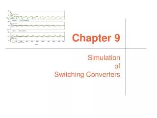
Example 4.5 • Draw circuit as shown in figure: • R, L, C are all from “breakout.olb” • Define models RMOD, LMOD, andCMOD as shown in the figure on thebottom. Use the new models in the circuit. • Define initial conditions (IC) of L and C in the property editor. • The PWL voltage source is the VPWL from “source.olb”. The VPWL source parameters are: (T1=0, T2=10ns, T3=2ms, V1=0, V2=10, V3=10) • Create a new simulation profile • Analysis type is: Time Domain (Transient). Run to time: 1ms, Max step size: 5us. • Temperature (sweep): Run at 50°C. • Obtain the simulation result in the figure: Figure 4.5.1 EENG 2920, Class 3 Figure 4.5.2
Example 4.6 • Repeat Example 4.5 withthe following difference: • L1 has no initial condition • The initial condition for C1 has been changed to -4V. • Notice that the response is completely different from Example 4.5, because the initial conditions of L and C are different. Figure 4.6.1 Figure 4.6.2 EENG 2920, Class 3