Download
1 / 12
120 likes | 258 Views
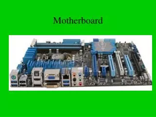
PR-DLS Motherboard Training for TSD & RMA engineers. PR-DLS Specification - 1. Processor. Supports SMP (Symmetrical Multi-Processor) dual processors MPS (Multi-Processor Specification) rev 1.4 compliant Supports 604-pin INT -mPGA Intel Foster / Prestonua / Gallatin up to 2.4G+Hz

E N D
PR-DLS Specification - 1 Processor • Supports SMP (Symmetrical Multi-Processor) dual processors • MPS (Multi-Processor Specification) rev 1.4 compliant • Supports 604-pin INT-mPGAIntel Foster / Prestonua / Gallatin up to 2.4G+Hz • FSB 400Mhz support Chipset • RCC Grand Champion LE Server 2.0 (GCLE) • RCC Champion South Bridge 5.0 (CSB5) • RCC Champion IO Bridge X2 (CIOBX2) • Support PC1600 DDR SDRAM interface (Registered DIMM only) • Support PCI to PCI Transfer • Support two channel 64-bit/133Mhz PCI bus
PR-DLS Specification - 2 System Memory • 6 x 184-pin DIMM sockets support 128MB to 2 GB PC1600 registered DIMM module • Two-way Interleaved (144bit) ECC DIMM Slot • 1 x PCI-32bit/33Mhz 5V slot • 5 x PCI-64bit/133Mhz 3V slots
1 x PS/2 Keyboard Port, 1 x PS/2 Mouse Port • 1 x Floppy Port (Up to 2.88MB, 3 Mode) • 2 x ATA-100 IDE connectors • 2 x external USB Ports (Support Hot-Plug Function) • 2 x on-board USB connectors • 1 x external Serial Port, 1 x internal Serial Port connector • 1 x Parallel Port ( ECP, EPP Port) • 1 RJ-45 10/100/1000 LAN ports /w LED • 1 RJ-45 10/100 LAN ports /w LED • 1 15-pin VGA port • 2 68-pin Ultra160/320 SCSI connector • 2 Feature connector (for IPMI solution) PR-DLS Specification - 3 Onboard I/O
PR-DLS Specification - 4 Onboard IDE • Dual channel Bus Master IDE ports supports ATA-100, • Multi-Word DMA Mode 2, PIO Mode 3/4 • ATAPI IDE CD-ROM, CD-R, CD-RW and LS-120 Supported Onboard SCSI • Dual Channel Ultra160/320 SCSI • LSI 1010R/1030 64-bit/66Mhz/133Mhz SCSI controller Onboard LAN • 1x Intel 82544GC LAN Chip on Board • Support 10/100/1000Mb/sec • 1x Intel 82551 LAN Chip on Board • Support 10/100Mb/sec
PR-DLS Specification - 5 Special Features • System Auto Speed Down While CPU Overheat • Wake-up on Ring, LAN • Previous State/Off Setup of AC Recovery from Power Failure BIOS • 4Mbit Flash memory • Award BIOS with Enhanced Server, ACPI, DMI, Green, PnP Features Plus, VGA & SCSI BIOS • Year 2000 Test Approved Board Size • EATX (12” x 13”)
PR-DLS Clock Generator Circuit - 1 FB_IN DIMM x 6 CLK Gen ICS 9248-152 CPU CPUCLK 1,2 (100MHz) DCLK 0,1,2,3,4,5 CLOCK BUFFER 93701 RCC GCLE CMICCK(100MHz) LEDDRCK (100MHz) 32.768K 25Mhz LAN 87417 48MHz RCC CSB5 CSB514M 559CLK 14MHz ICS 9112-26 ASIC14M CSB5CK SIOCK ASIC AS99127 PCI6CK CLOCK BUFFER 2510 VGAPCLK VGA14M ATI RAGE XL 33MHz 33MFIN
PR-DLS Clock Generator Circuit -2 PCI1PCLK CLK Gen ICS 9248-152 CIOBX22CK RCC CIOBX2 B Intel 82544GC GIGAPCLK P3,P4CLKFB CLOCK BUFFER 2510 33MHz PCI x 3 P1,P2CLKFB RCC CIOBX2 A CIOBX2CK PCI2,3,4CLK PCI5CLK 40MHz SCSIPCLK SCSI LSI 1010R
Device/Slot Bus No. Device No./IDSEL INTA INTB INTC INTD 10/100 LOM 0 AD18 PCIIRQ2# PCI VGA 0 AD19 PCIIRQ30# PCI6 0 AD20 PCIIRQ10# PCIIRQ27# PCIIRQ28# PCIIRQ29# PCI2 1 AD18 PCIIRQ4# PCIIRQ15# PCIIRQ16# PCIIRQ17# PCI3 1 AD19 PCIIRQ5# PCIIRQ18# PCIIRQ19# PCIIRQ20# PCI4 1 AD20 PCIIRQ8# PCIIRQ21# PCIIRQ22# PCIIRQ23# PCI5 2 AD18 PCIIRQ9# PCIIRQ24# PCIIRQ6# PCIIRQ7# LSI 53C1010R/1030 2 AD20 PCIIRQ6# PCIIRQ7# 10/100/GbE LOM 3 AD18 PCIIRQ3# PCI1 4 AD18 PCIIRQ1# PCIIRQ12# PCIIRQ13# PCIIRQ14# PR-DLS PCI IRQ Routing Table