Download
1 / 33
330 likes | 403 Views
Electrical Engineering 2. Lecture 3. Microelectronics 2. Dr. Peter Ewen. (Room G08, SMC; email - pjse). ELECTRON ENERGY - THE ELECTRON-VOLT (eV) THE ENERGY ACQUIRED BY AN ELECTRON IN PASSING THROUGH A POTENTIAL DIFFERENCE OF 1V E = q V 1eV = 1.6 x 10 -19 J. METALLIC BONDING

E N D
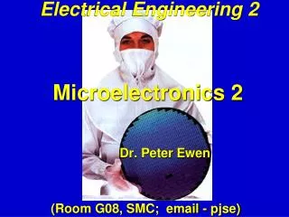
Electrical Engineering 2 Lecture 3 Microelectronics 2 Dr. Peter Ewen (Room G08, SMC; email - pjse)
ELECTRON ENERGY - THE ELECTRON-VOLT (eV) THE ENERGY ACQUIRED BY AN ELECTRON IN PASSING THROUGH A POTENTIAL DIFFERENCE OF 1V E = q V 1eV = 1.6 x 10⁻¹⁹ J
METALLIC BONDING • Valence electrons are free to move through solid. • In monovalent metals each atom contributes one free valence electron at room temp. • COVALENT BONDING • Valence electrons shared with adjacent atoms. • In Si & Ge each atom shares 2 valence electrons with each of 4 neighbouring atoms – i.e. there are 4 covalent bonds. +ve ion cores cloud of -ve electrons
At 0K all the valence electrons are firmly held in the bonds electrons Fig. 15: Crystal structure of silicon silicon atoms
As temperature rises, some of the bonding electrons break free electrons Fig. 15: Crystal structure of silicon silicon atoms
Fig. 16 ELECTRON ENERGY BANDS Allowed bands Forbidden band Electron energy Allowed band Allowed band 2 4 1 N Number of close atoms Isolated atom
Fig. 16 ELECTRON ENERGY BANDS Conduction band Electron energy Valence electrons Valence band 1 2 4 N Number of close atoms Isolated atom
MetalSemiconductorInsulator Fig. 17 Conduction Band (CB) CB CB Valence Band (VB) Eg (~1 eV) Electron energy VB Eg The ENERGY GAP, Eg, corresponds to the energy required to break a covalent bond in the solid. VB Mainly empty energy levels Mainly occupied energy levels
ELECTRON ENERGY As temperature increases, structure expands Applying pressure compresses structure Energy levels of the Isolated atom Equilibrium spacing INTERATOMIC SPACING Fig 19: Variation of the energy bands with interatomic spacing for silicon (and also germanium and carbon).
LECTURE 3 Holes • Intrinsic and extrinsic semiconductors • Resistivity • Temperature coefficient of resistance (TCR)
- + Semiconductor Electron-hole pair Si Si Si -ve +ve Fig. 20a Electric field +ve charge associated with vacancy the vacancy is mobile the vacancy acts like a mobile +ve charge Fig. 20b
INTRINSIC SEMICONDUCTORS Pure semiconductors are termed “intrinsic”: Si Si Si n = p = ni n – free electron concentration; p – hole concentration ni – intrinsic carrier concentration (N.B. ni ≠ n + p) At 300K: ni= 1.5x10¹⁶ m-3 for Si ni= 2.5x10¹⁹ m-3 for Ge
Strong Bond strength Weak Fig. 18: Variation of energy gap with interatomic spacing for Group IV elements.
The intrinsic carrier concentration in a semiconductor is 4x10¹⁶ m-3. Which one of the statements below is true? A. The total carrier concentration is 4x10¹⁶ m-3. B. The concentration of electron-hole pairs is 8x10¹⁶ m-3. C. The electron concentration is 2x10¹⁶ m-3. D. The total carrier concentration is 8x10¹⁶ m-3.
Eg C.B. Fig. 21 RECOMBINATION GENERATION V.B. CARRIER LIFETIME - : 10-9 < < 10-6 s
n-type pentavalent donor atoms p-type trivalent acceptor atoms EXTRINSICSEMICONDUCTORS Substitutional impurities – they can be incorporated into the semiconductor lattice without distorting it. Typical doping concentrations: 1020 – 1026 m-3
C.B. Donor levels Energy ~0.01 eV V.B. Fig. 22a Si Si Si As n-type Si Donor atom Si
C.B. Energy ~0.01 eV Acceptor levels V.B. Fig. 22b Si Si Si B p-type Si Acceptor atom Si
i i i i i Fig. 23: Typical range of conductivities/resistivities for metals insulators and semiconductors.
i i i i i Fig. 23: Typical range of conductivities/resistivities for metals insulators and semiconductors.
Fig. 24 Temperature Coefficient of Resistance def
5. TCR for a metal The resistance of a copper wire increases approximately linearly from 1.7x10⁻⁸at 300K to 3.7x10⁻⁸at 600K. What is the TCR of copper at 300K?
5. TCR for a metal For an arbitrary material with +ve TCR: If R T: Resistance/R Resistance/R ΔR R(T1) R(T1) ΔT T1 Temperature/T T1 Temperature/T For linear variation of R with T: The TCR at a given temperature T1 is given by: where dR/dT is the gradient of the curve at T1. 1.7x10⁻⁸at 300K 3.7x10⁻⁸at 600K
6. Effect of TCR on semiconductor resistance Resistors in an IC can be made simply by doping a region of the semiconductor appropriately. If a resistor made this way has a resistance of 100 and a TCR of -2.8x10⁻²/K at 300K, what is its resistance at 320K, assuming a linear variation? Iout Iin n-type region Region produced by implantation or diffusion of dopant p-type wafer
6. Effect of TCR on semiconductor resistance For a linear variation of R with T:
7. Temperature coefficient of resistivity Show that if the dimensions of a sample do not depend significantly on temperature, the temperature coefficient of resistance (R) is the same as the temperature coefficient of resistivity (ρ). Show that this will be the case for copper, which has a thermal expansion coefficient of 1.7x10⁻⁵/K.
7. Temperature coefficient of resistivity If l and A do not depend significantly on temperature:
What happens for copper, with a thermal expansion coefficient of 1.7x10⁻⁵ K-1 ? We need to show that l/A doesn’t change significantly with temperature. When a material expands, its dimensions increase by a factor (1+α∆T), where αis the thermal expansion coefficient, e.g. for its length, l: Consider a temperature rise of, say, 100K: Thus the ratio l/A hardly changes over this temperature range and so the temperature coefficients of resistance and resistivity will be the same.
SUMMARY • HOLES • The vacancy left in a bond when an electron breaks free is termed a HOLE. • A hole behaves like a mobile positive charge. • Holes are just as important as electrons in conduction processes in semiconductors.
INTRINSIC SEMICONDUCTORS • The pure semiconductor is termed INTRINSIC. • In the intrinsic semiconductor electrons and holes are created in pairs by bond-breaking – electron-hole pair generation • n = p = nini is the intrinsic carrier concentration. • Because the reverse process (recombination) is possible, mobile carriers have a finite life-time, .
EXTRINSIC SEMICONDUCTORS • Extrinsic semiconductors are doped with group 3 or group 5 atoms: pentavalent atoms donor impurities n-type • trivalent atoms acceptor impurities p-type • Donor electrons only require ~ 0.01eV of energy to break free and so at room temperature all donor electrons are in the conduction band. • Similarly, acceptor impurities create holes in the valence band.
C.B. C.B. Energy ~0.01 eV Donor levels Energy Acceptor levels ~0.01 eV V.B. V.B. • Donor impurities give rise to a set of energy levels in the gap, just below the conduction band - the donor levels. • Acceptor impurities give rise to a set of energy levels in the gap, just above the valence band - the acceptor levels.
EFFECT OF TEMPERATURE ON RESISTIVITY • As temperature increases: R for metals but R for intrinsic semiconductors and insulators R, R or stays constant for extrinsic semiconductors. • Temperature Coeficient of Resistance: