Download
1 / 38
410 likes | 619 Views
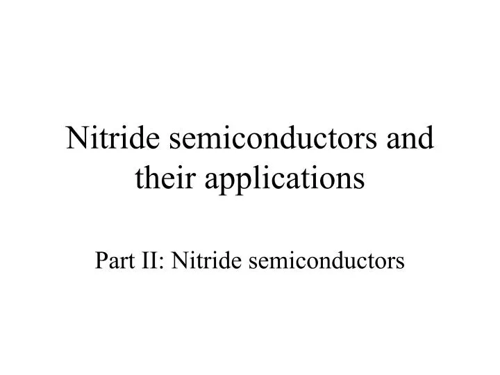
Nitride semiconductors and their applications. Part II: Nitride semiconductors. Nitride papers published. Nitride-based semiconductors. A III-V semiconductor in which N is one of the elements. Examples include AlN, GaN, InN, and alloys such as Al x Ga 1-x N.

E N D
Nitride semiconductors and their applications Part II: Nitride semiconductors
Nitride-based semiconductors • A III-V semiconductor in which N is one of the elements. Examples include AlN, GaN, InN, and alloys such as AlxGa1-xN. • These materials have high melting points (strong bond with N) and a wide span of bandgaps (from 0.7 eV for InN to 3.4 eV for GaN to 6.2 eV for AlN).
Applications • High-temperature, high-power electronics • Ultraviolet (UV) radiation detectors • feedback systems in furnaces and engines • solar-blind missile early warning systems • astronomical applications • LEDs and LDs
Blue LEDs and LDs • Full color day-visible displays • Energy efficient lighting • Traffic lights, replace every 6 months, LEDs, every 5-10 years (60,000 hours) • Consumer lighting applications. • Higher storage density on optical media (>50 GB on a single DVD) • Faster on-time • Fluorescent photosensitizers accumulate preferentially in cancerous cells.
Short history 1971 GaN LED demonstrated (Pankove) 1986 “High” quality GaN grown (Akasaki) 1988 P-type GaN grown (Akasaki); Nakamura starts work on GaN 1990 Two-flow MOCVD system developed (Nakamura) 1991 High quality p-type GaN grown; first pn-junction GaN LED created 1992 ZnSe-CdZnSe blue laser developed (3M) 1993 Commercial blue GaN LEDs introduced (Nichia) 1996 Room temperature nitride LDs developed (Nichia) 1999 Commercial nitride LDs introduced (Nichia) 2004 SONY markets blue laser DVD writers (23 GB/layer)
Nitride problems 1. Inability to grow good quality crystals 2. Inability to grow p-type crystals
Crystal quality • Problem: No lattice matched substrates, high growth temperature results in convection currents • Sapphire is closest but is 15% off. • SiC is too expensive • MOCVD growth too fast for good control (few mm/min) • Solution: Buffer layers, new growth system • First grow GaN or AlN buffer layer • Two-flow MOCVD system • Still many many dislocations in material (1010 cm-2) but dislocations don’t matter?
Two-flow MOCVD Nakamura, Harada, and Seno, J. Appl. Phys 58, 2021 (1991)
Buffer layer Dislocation High quality GaN Low quality GaN (0.2 mm) AlN or GaN buffer layer (0.05 mm) Substrate
p-type GaN • Problem: No one could dope GaN p-type • Solution: • At first, LEEBI (Low Energy Electron Beam Irradiation) • Later, annealing at 700°C in non H-containing gas • Hydrogen was passivating the acceptors!
Factors leading to success • Small bureaucracy (N. Ogawa and S. Nakamura) • A 3.3 M$ USD gamble (1.5% of annual sales) • Large companies tend to be conservative, both in funds and in research outlook
Current research on nitrides • Fundamental physics • Improving crystal quality (still very poor) • Ultraviolet lasers • Lattice matching with quaternary alloys (AlGaInN) • Nitride heterostructures and accompanying applications
Heterostructure usefulness Charge carriers are spatially separated from the (now) ionized impurity atoms, leading to higher carrier mobilities. Electrons form a 2-Dimensional Electron Gas (2-DEG).
Research questions • Even undoped, carrier densities in AlGaN/GaN heterostructures is 10 to 100 times larger than those in similar (AlGaAs/GaAs) systems.What is the source of these carriers? • Carrier mobilities in AlGaN/GaN heterostructures are 10 to 100 times lower than in the AlGaAs/GaAs system.What are the principle mechanisms limiting the mobility?
Origin of carriers Current theory: surface donor defects on AlGaN Concentration of surface defects and transfer of electrons to GaN well is enhanced by strain-induced electric field.
Pseudomorphic growth AlGaN AlGaN/GaN interface • GaN and AlN have ~2.5% lattice mismatch • Grown on polar c-axis • Spontaneous and induced piezoelectric fields are present GaN lattice matched non-lattice matched
Band structure • When AlGaN barrier is thick enough to pull defect level above bottom of GaN well, electrons begin to transfer to well. • Formation energy of donor defects is reduced because electrons can drop to lower energy level by transferring to GaN well
Comparison with experiment Smorchkova et al., J. Appl. Phys 86, 4520 (1999)
Transport properties Semiconductor with no applied field: • Electrons move randomly with an average velocity of zero • Mean time between electron-electron collisions is t. With an applied field: • Electrons have an acceleration of a = eE/m* • Average velocity of electrons is at, parallel to field. The mobility is a measure of how easily charge carriers respond to an applied electric field.
Limiting factors Scattering mechanisms • Coulomb fields • Phonons • Alloy disorder
Coulomb scattering Electrons are affected by the long-range Coulomb fields of randomly distributed ionized donor atoms. • Thicker barriers move ionized surface donors further away from carriers. • Large 2-DEG densities screen the effect of these Coulomb fields.
Phonon scattering Phonons are lattice vibrations in a crystal. Acoustic phonons • Both types of atoms move “in-phase” • Low energy vibrations Optical phonons • Atoms of different types move “out-of-phase” • High energy vibration
Phonon scattering • Phonons scatter carriers by creating small fluctuating dipoles between atoms (piezoelectric mode). • Phonons scatter carriers by disturbing the periodicity of the crystal lattice (deformation potential mode).
Alloy disorder • Electron wavefunction penetrates into AlGaN barrier. • Al and Ga atoms are distributed randomly in AlGaN • Randomly varying potential scatters electrons.
Improving the mobility Strategies: • Reduce 2-DEG density • Smaller Al alloy fractions • Thinner barriers (Highest mobility heterostructures have Al fractions of ~10% and barrier thicknesses of ~130 Å) • Reduce alloy disorder scattering • AlN spacer
Conclusions • Nitride-based semiconductors are a promising field for a wide variety of new technological applications. • 2-DEG mobilities are limited by two factors: • Coulomb scattering (N < 2 x 1012 cm-2) • Alloy disorder scattering (N > 4 x 1012 cm-2) • We predict maximum low temp mobilities of 105 cm2/V s without a AlN spacer. • Using a AlN spacer seems a promising way to improve the conductivity of nitride heterostructures.
Subband structure Confining potential results in quantized energy levels. Trial wavefunction
Comparison with experiment Smorchkova et al., J. Appl. Phys 86, 4520 (1999)
Comparison with experiment Smorchkova et al., J. Appl. Phys 86, 4520 (1999)