Download
1 / 1
20 likes | 107 Views
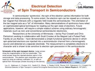
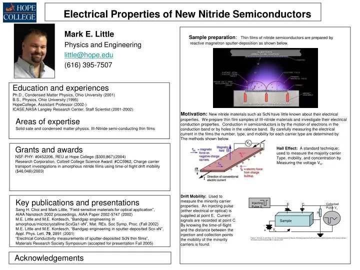
Injecting Pulse V i. E. C. Collected Pulse V c. R b. Sample. -. +. V s. Figure 1: Sconza, A. and Torzo, G. “An improved version of Haynes-Shockley experiment with electrical or optical injection of the excess carriers” American Journal of physics 68 (1) January 2000.

E N D
Injecting Pulse Vi E C Collected Pulse Vc Rb Sample - + Vs Figure 1: Sconza, A. and Torzo, G. “An improved version of Haynes-Shockley experiment with electrical or optical injection of the excess carriers” American Journal of physics 68 (1) January 2000 Electrical Properties of New Nitride Semiconductors Mark E. Little Physics and Engineering little@hope.edu (616) 395-7507 Sample preparation:Thin films of nitride semiconductors are prepared by reactive magnetron sputter-deposition as shown below. Photograph Education and experiences Ph.D., Condensed Matter Physics, Ohio University (2001) B.S., Physics, Ohio University (1995) HopeCollege, Assistant Professor (2002-) ICASE,NASA Langley Research Center, Staff Scientist (2001-2002) Motivation:New nitride materials such as ScN have little known about their electrical properties. We prepare thin film samples of III-nitride materials and investigate their electrical conduction properties. Conduction in semiconductors is by the motion of electrons in the conduction band or by holes in the valence band. By carefully measuring the electrical current in the films the number, type, and mobility for each carrier type are determined by The methods shown below. Areas of expertise Solid sate and condensed matter physics. III-Nitride semi-conducting thin films Grants and awards NSF-PHY: #0452206, REU at Hope College ($300,867)(2004) Research Corporation, Cottrell College Science Award: #CC5962, Charge carrier transport investigations in amorphous nitride films using time-of flight drift mobility ($46,048)(2003) Hall Effect: A standard technique; used to measure the majority carrier Type, mobility, and concentration by Measuring the voltage VH. • Drift Mobility: Used to • measure the minority carrier • properties. An injecting pulse • (either electrical or optical) is • supplied at point E. Current • signals are recorded at point C. • By knowing the time-of-flight • and the distance between the • injection and collection points • the mobility of the minority • carriers is found. Key publications and presentations Sang H. Choi and Mark Little, “Field-sensitive materials for optical application”, AIAA Nanotech 2002 proceedings, AIAA Paper 2002-5747 (2002) M.E. Little and M.E. Kordesch, “Bandgap engineering in amorphous/microcrystalline ScxGa1-xN”, Mat. REs. Soc Symp. Proc. (Fall 2002) M.E. Little and M.E. Kordesch, “Bandgap engineering in sputter-deposited Scx-xN”, Appl. Phys. Lett. 79, 2891 (2001) “Electrical Conductivity measurements of sputter-deposited ScN thin films”, Materials Research Society Symposium (accepted for presentation Fall 2005) Acknowledgements