Download
1 / 14
150 likes | 304 Views
Quantum Transport Simulation in DG MOSFETs using a Tight Binding Green’s function Formalism. M. Bescond, J-L. Autran, M. Lannoo. 4 th European Workshop on Ultimate Integration of Silicon, March 20 and 21, 2003. Outline. Overview of the problem Device considered

E N D
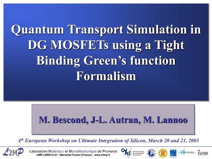
Quantum Transport Simulation in DG MOSFETs using a Tight Binding Green’s function Formalism M. Bescond, J-L. Autran, M. Lannoo 4th European Workshop on Ultimate Integration of Silicon, March 20 and 21, 2003
Outline • Overview of the problem • Device considered • Theory: Tight Binding Green’s function formalism • Results and discussion • Conclusion
E(k) Parabolic approximation of an homogeneous medium Parabolic approximation of a finished system of atoms 0 k Overview of the problem • Device dimensions scale into the nanometer regime. • The Green’s function formalism represents a basic method to describe the quantum behavior of the transistors : capacity to describe interactions and semi-infinite contact (source, drain). • However, most of the studies consider this formalism in the EMA, whose validity in the nanometer scale is debatable :
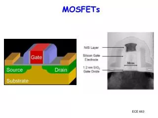
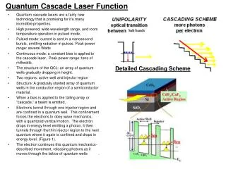
Device considered • Single Atomic conduction channel DG MOSFET. • Mixed-mode approach : • The axis source-channel-drain is represented by an atomic linear chain treated in tight binding (1). • The other parts of the system are classically treated from a dielectric point of view. (1) M. Bescond, M. Lannoo, D. Goguenheim, J-L. Autran, Journal of Non-Cristalline Solids (2003) in press.
Source Channel Drain E (eV) E (eV) EFS EFD VDS 0.11 eV E (eV) X Device considered • Band profile versus position : • Hypothesis : • Source and drain are considered as metallic reservoirs. • We consider a negative Schottky barrier of –0.11 eV.
Energy Hamiltonian Self energies(2) AS = GSG+ AD = GDG+ Spectral functions Tight binding Green’s function formalism • Retarded Green’s function :(2) S. Datta, Superlatt. Microstruct., 28, 253 (2000). One defines and Electron density can be computed as : f : Fermi-Dirac distribution
Tight binding Green’s function formalism • The current : • The device is virtually cleaved into two regions : • The transmitted current I through the plane separating the two parts is : , where Q is the charge density of the system.
Tight binding Green’s function formalism • In the tight binding set, hamiltonian operator has the following form : • The associated retarded Green’s function of the uncoupled system is : • The final expression of the current is : Include the self energies of the semi-infinite source and drain. Coupling matrix -2in = g-g* =(I-gVgV))-1 Tr1 trace restricted to part 1
Simulation code : Electron density profiles : Electrostatic Potential + Electron density Poisson 2D Self-consistent coupling New Electrostatic Potential Green New Electron density CURRENT Results and Discussion
Results and discussion • IDS versus VG at two different temperatures : • Tunneling current affects : - the magnitude of the current in the subthreshold region, - the quantitative shape of the curve.
VDS= 0.4 V Results and discussion • IDS (VG) for several values of the channel length : • For a 20 nm device, the curve has a nearly perfect slope of 60 mV/decade. • In smaller devices, the increase of the subthreshold current is due to electron tunneling through the ‘bump’ of the electric potential profile.
Results and discussion • IDS vs VDS. Dashed line represents the current obtained with a quantum of conductance G0 = 2e²/h (3). • In thin channels, the conductance is quantified in units of G0. • Saturation shows up only when the electron potential energy maximum in the channel is suppressed by positive gate voltage, and is due to the exhaustion of source electrons. Reflections due to the drop voltage (3) R. Landauer, J. Phys. :Condens. Matter, 1, 8099 (1989).
Results and discussion • Transmission coefficient for VG = 0.7 V : • Even if injected ballistic particles transmit freely from source to drain without channel potential barrier, reflections due to the drop voltage VDS still exist. • Transparency attenuation is all the more pronounced as the applied voltage VDS increases .
Conclusion • Single conduction channel MOSFET device using tight binding Green’s function formalism has been simulated. • « Tunneling transistor » : tunneling effect changes the overall shape of the current characteristics : the subthreshold curve is no longer exponential. • Even in the strong-tunneling regime the transistor is still responsive to gate voltage. • Because of the decrease of the transverse number, the resonant level energies of the channel have to be determined with a high precision. Next step : include the 3D silicon atomic structure.