Download
1 / 41
570 likes | 1.11k Views
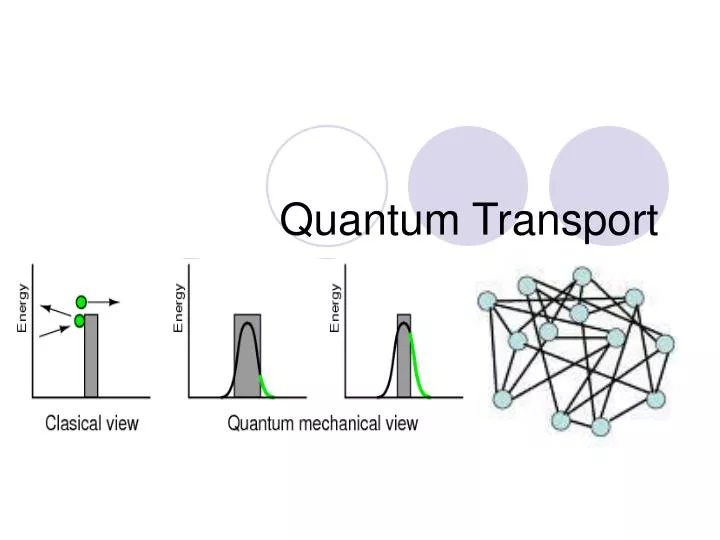
Quantum Transport. Outline:. What is Computational Electronics? Semi-Classical Transport Theory Drift-Diffusion Simulations Hydrodynamic Simulations Particle-Based Device Simulations Inclusion of Tunneling and Size-Quantization Effects in Semi-Classical Simulators

E N D
Outline: • What is Computational Electronics? • Semi-Classical Transport Theory • Drift-Diffusion Simulations • Hydrodynamic Simulations • Particle-Based Device Simulations • Inclusion of Tunneling and Size-Quantization Effects in Semi-Classical Simulators • Tunneling Effect: WKB Approximation and Transfer Matrix Approach • Quantum-Mechanical Size Quantization Effect • Drift-Diffusion and Hydrodynamics: Quantum Correction and Quantum Moment Methods • Particle-Based Device Simulations: Effective Potential Approach • Quantum Transport • Direct Solution of the Schrodinger Equation (Usuki Method) and Theoretical Basis of the Green’s Functions Approach (NEGF) • NEGF: Recursive Green’s Function Technique and CBR Approach • Atomistic Simulations – The Future • Prologue
Transport Properties of system/device using Green’s functions formalism • Low field transport • Linear response theory (ASU) • High field transport • Bulk systems – Airy approach (Rita Bertoncini, ASU, PhD Thesis) • Devices: • Recursive Green’s Functions Approach (ASU, Purdue) • CBR Approach (ASU, WSI, Purdue)
Linear Response Theory • Only the retarded Green’s function is needed as it includes the collisional broadening of the states • In the ASU’s simulator for low-field mobility calculation in silicon inversion layers, strained-Si layers and InGaAs/InAlAs heterostructures the following features have been implemented: • Realistic treatmet of scattering within the self-consistent Born approximation • Modification of the density of states function is accounted for due to the collisional broadening of the states and the intersubband scattering • Random phase approximation in its full implementation is included to properly treat static screening of Coulomb and Interface-Roughness scattering • Bethe-Salpether integral equation is solved in the calculation of the conductivity • Excellent agreement is obtained with measured low-field mobility data in silicon inversion layers and predictions were made for the mobility behavior in Strained-Si layers and InGaAs/InAlAs heterostructures that were later confirmed with experimental measurements
Relevant Literature • D. Vasileska, P. Bordone, T. Eldridge and D.K. Ferry, “Calculation of the average interface field in inversion layers using zero-temperature Green’s functions formalism”, J. Vac. Sci. Technol. B 13, 1841-7 (1995). • P. Bordone, D. Vasileska and D.K. Ferry, “Collision duration time for optical phonon emission in semiconductors”, Physical Review B 53, 3846-55 (1996). • D. Vasileska, T. Eldridge and D.K. Ferry, “Quantum transport: Silicon inversion layers and InAlAs-InGaAs heterostructures”, J. Vac. Sci. Technol. B 14, 2780-5 (1996). • D. Vasileska, P. Bordone, T. Eldridge and D. K. Ferry, “Quantum transport calculations for silicon inversion layers in MOS structures”, Physica B 227, 333-5 (1996). • D. Vasileska and D. K. Ferry, “Scaled silicon MOSFET’s: Part I - Universal mobility behavior”, IEEE Trans. Electron Devices 44, 577-83 (1997). • G. Formicone, D. Vasileska and D.K. Ferry, “Transport in the surface channel of strained Si on a relaxed Si1-xGex substrate”, Solid State Electronics 41, 879-886 (1997).
Is Strain Beneficial in Nanoscale MOSFETs With High Channel Doping Densities?
High Field Transport in Devices:Recursive Green’s Functions Approach • The most complete 1D transport in resonant tunneling diodes (RTDs) that operate on purely quantum mechanical principles was accomplished with the NEMO1D Code • The NEMO 1D Code was developed by Roger Lake, Gerhard Klimeck, Chris Bowen and Dejan Jovanovich while working at Texas Instruments/Raytion • It solves the retarded Green’s function (spectral function) in conjuction with less-than Green’s function (occupation function) self-consistently • References for NEMO1D: • Roger. K. Lake, Gerhard Klimeck, R. Chris Bowen, Dejan Jovanovic, Paul Sotirelis and William R. Frensley,"A Generalized Tunneling Formula for Quantum Device Modeling",VLSI Design, Vol. 6, pg 9 (1998). • Roger Lake, Gerhard Klimeck, R. Chris Bowen and Dejan Jovanovic,"Single and multiband modeling of quantum electron transport through layered semiconductor devices", J. of Appl. Phys. 81, 7845 (1997).
The Philosophy Behind the Recursive Green’s Function Approach K. B. Kahen, Recursive-Green’s-function analysis of wave propagation in two-dimensional nonhomogeneous media, .Phys. Rev. E 47, 2927 - 2933 (1993).
where closed system Hamiltonian , self-energy matrix where describes closed system (decoupled device) High Field Transport in Devices:Contact Block Reduction Method The retarded Green’s function of an open system: The Dyson equation, To determine Green’s function of an open system we need to invert a huge matrix D. Mamaluy, D. Vasileska, M. Sabathil, T. Zibold, and P. Vogl, “Contact block reduction method for ballistic transport and carrier densities of open nanostructures”, Phys. Rev. B 71, 245321 (2005).
of an open system in CBR formalism: • The left upper block fully determine the transmission function • The left lower block determines density of states, charge density etc. Retarded Green’s Function C is the contact portion of the where, index D denotes the interior device region index C denotes the contact ( boundary ) region All elements of GR can be determined from inversion of small matrixAC
Transmission Function and Local Density of States Calculation • Transmission Function • CBR Formalism • Local Density of States Function • CBR Formalism
Properties of Widely Acceptable 2D Simulators H. R. Khan, D. Mamaluy and D. Vasileska, “Approaching Optimal Characteristics of 10 nm High Performance Devices” a Quantum Transport Simulation Study of Si FinFET, IEEE Trans. Electron Devices, Vol. 55(1), pp. 743-753 (2008). H. R. Khan, D. Mamaluy and D. Vasileska, “Simulation of the Impact of Process Variation on the Optimized 10-nm FinFET”, IEEE Transactions Electron Dev. Vol. 55(8), pp. 2134 – 2141, August 2008.
ON-State Electron density along the dotted line VGS=0.2, VDS=0.4V Electron density (TG) > electron density (DG)
Atomistic Simulations – The Future of Nano-Devices • Examples of devices for which atomistic simulations will be necessary include: • Devices in which local Strain exists • Alloy Disorder has to be properly described • Group of Gerhard Klimeck, Purdue University, West Lafayette, IN, USA • Group of Aldo di Carlo, Tor Vergata, Rome, Italy.
Why Tight-Binding ? • Allows us to describe the band structure over the entire Brillouin zone • Relaxes all the approximations of Envelope Function approaches • Allows us to describe thin layer perturbation (few Å) • Describes correctly band mixing • Gives atomic details • The computational cost is low • It is a real space approach • Molecular dynamics • Scalability (from empirical to ab-initio)
Scalability of TB approaches Empirical Tight-Binding Hamiltonian matrix elements are obtained by comparison of calculated quantities with experiments or ab-initio results. Very efficient, Poor transferability. Semi-Empirical Hartree-Fock Methods used in the chemistry context (INDO, PM3 etc.). Medium transferability. Density Functional based Tight-Binding (DFTB, FIREBALL, SIESTA) DFT local basis approaches provide transferable and accurate interaction potentials. The numerical efficiency of the method allows for molecular dynamics simulations in large super cells, containing several hundreds of atoms.
The sp3s* Hamiltonian [Vogl et al. J. Phys. Chem Sol. 44, 365 (1983)] In order to reproduce both valence and conduction band of covalently bounded semiconductors a s* orbital is introduced to account for high energy orbitals (d, f etc.)
The sp3d5s* Hamiltonian[Jancu et al. PRB 57 (1998)] Many parameters, but works quite well !
Tight-Binding sp3d5s* model for nitrides Ab-Inito Plane Wave DFT-LDA Band Structure for GaN Wurtzite TB Wurtzite GaN Band Structure Nearest-neighbours sp3d5s* tight-binding parametrization for wurtzite GaN, AlN and InN compare well with Ab-Initio results.
H= H= P P P Boundary conditions Periodic After P planes the structure repeats itself. Suitable for superlattices Finite chain After P planes the structure end. Suitable for quantum wells Open boundary conditions After P planes there is a semiinfinite crystal Suitable for current calculations ∞ ∞ BULK BULK
Where do we put the atoms ? To describe the electronic and optical properties of a nanostructure we need to know where the atoms are. • We know “a priori” the atom positions (for example X-ray • information) 2) We need to calculate the atomic positions Simple analytic espressions Full calculation Continuum theory Classical calculations Atomistic (Valence Force Field) Quantum calculation
as a0 as a0 as as as as as Example: Strain and Pseudomorphic growth An epitaxial layer is grown, on a substrate with different lattice constant. The epilayer deforms (strain) as Strain tensor
z, [0001] Strain in a AlGaN/GaN Nanocolumn Calleja’s pillars 20nm Al0.28Ga0.72 N GaN
AlGaN/GaN Nanocolumns Potential The Poisson equation piezo-electric polarization pyro-electric polarization piezo-electric moduli tensor
2) Virtual crystal approximation A new crystal is defined with averaged properties (P) P(AxB1-xC)=x P(AC) + (1-x) P(BC) How do we describe alloys ? Usually, tight-binding parameterizations are made for single elments and binary compounds (Si, Ge, GaAs, InAs etc.). However, nanostructure are usually build by using also ternary (AlGaAs etc.) and quatrnary (InGaAsP etc.) alloys. 1) Supercell calculations A0.5B0.5C Average over an ensamble of configurations 3) Other methods (Modified VCA, CPA, T-matrix etc.)
Schrodinger Poisson Self-Consistent Tight-Binding Charge transfer is important in semiconductor nanostructures. Self-consistent solution of Schredinger and Poisson equations are common in envelope function approaches Tight-binding allows for a full (with all the electrons) self-consistent solution of the nanostructure problem Full self consistent approach only suitable for small systems likemolecules Self-consistent approach for only the free charge With the aim of Self-Consistent treatment of external electrostatic potential, Tight-Binding can be applied to semiconductor device simulations.
x y z Self-Consistent Tight-Binding [A. Di Carlo et. al., Solid State Comm. 98, 803 (1996); APL 74, 2002 (1999)] The electron and hole densities in each 2D layer are given by: The influence of free carrier charge redistribution and macroscopic polarization fields are included by solving the Poisson equation: boundary conditions +
Summary • Linear response and solution of the Beth-Salpether equation in conjunction with the Dyson equation for the retarded Green’s function is useful when modeling low-field mobility of inversion layers • When modeling high field transport both Dyson equation for the retarded Green’s function and the kinetic equation for the less-than Green’s function have to be solved self-consistently • CBR approach and recursive Green’s function method have both their advantages and their disadvantages • When local strains and stresses have to be accounted for in ultra-nano-scale devices then atomistic approaches become crucial
What are the lessons that we have learned? • Semi-classical simulation is still a very important part of Today’s semiconductor device modeling as power devices and solar cells (traditional ones) operate on semi-classical principles • Quantum corrections can quite accurately account for the quantum-mechanical size quantization effect which gives about 10% correction to the gate capacitance • For modeling ultra-nano scale devices one can successfully utilize both Poisson-Monte Carlo-Schrodinger solvers and fully quantum-mechanical approaches based on NEGF (tunelling + size quantization) • Full NEGF is a MUST when quantum interference effects need to be captured and play crucial role in the overall device behavior • For a subset of ultra-nano scale devices that are in the focus of the scientific community now, in which band-structure, local strain and stresses, play significant role, atomistic simulations are necessary.
Simulation Strategy for Ultra-Nano-Scale Devices Calibrate semi-empirical approaches with ab-initio band structure simulations 1000 atoms Parallel Computing Essential Perform BANDSTRUCTURE/TRANSPORT calculations on systems containing millions of atoms Millions of atoms
Atomistic Simulations Selected Literature • Mathieu Luisier and Gerhard Klimeck,"A multi-level parallel simulation approach to electron transport in nano-scale transistors", Supercomputing 2008, Austin TX, Nov. 15-21 2008. Regular paper - 59 accepted papers, 277. • Mathieu Luisier, Neophytos Neophytou, Neerav Kharche, and Gerhard Klimeck,"Full-Band and Atomistic Simulation of Realistic 40 nm InAs HEMT", IEEE IEDM, San Francisco, USA, Dec. 15-17, 2008, DOI : 10.1109/IEDM.2008.4796842, • Mathieu Luisier, and Gerhard Klimeck,"Performance analysis of statistical samples of graphene nanoribbon tunneling transistors with line edge roughness", Applied Physics Letters, Vol. 94, 223505 (2009), DOI:10.1063/1.3140505, • Mathieu Luisier, and Gerhard Klimeck, "Atomistic, Full-Band Design Study of InAs Band-to-Band Tunneling Field-Effect Transistors ", IEEE Electron Device Letters, Vol. 30, pp. 602-604 (2009), DOI:10.1109/LED.2009.2020442.