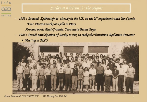
Download
1 / 13
130 likes | 246 Views
Update on the D0 Run IIb Silicon Upgrade for the Inner Layer Sensor PRR 8 August 03 George Ginther University of Rochester On behalf of the Run IIb Silicon Group. Detector Design. Six layer silicon tracker, divided into two radial groups and two barrels Inner layers: Layers 0 and 1

E N D
Update on the D0 Run IIb Silicon Upgrade for the Inner Layer Sensor PRR 8 August 03 George Ginther University of Rochester On behalf of the Run IIb Silicon Group
Detector Design • Six layer silicon tracker, divided into two radial groups and two barrels • Inner layers: Layers 0 and 1 • 18mm < R < 39mm • Axial readout only • 50/58 mm readout for L0/L1 • Assembled into one unit • Mounted on integrated support • Outer layers: Layers 2-5 • 53mm < R < 164 mm • Axial and stereo readout • 60 mm readout pitch • Stave support structure • Employs only single sided silicon • Three sensor sizes L0 (2 chip) L1 (3 chip) L2-L5 (5 chip) • All sensors have intermediate strips
Inner Layers • 12 sided carbon fiber support structures • Six sensors mounted on each side of the support structure L1 Support Structure Assembly Layer 0 pre-prototype with co-bonded grounding flex circuits
Hybrid 8’ Twisted Pair Cable 2’ Digital Cable Junction Card Sensor Analog Cable 8’ Twisted Pair Cable Interface with current DAQ system 2’ Digital Cable Junction Card Sensor Hybrid Adapter Card Readout Schematics Layers 1-5: Hybrids mounted directly on silicon Layer 0: Hybrids connected to sensors via analog cables(to address space and thermal constraints) SVX4 chips mounted on hybrids; employed in SVX2 readout mode to facilitate reuse of Run IIa higher level readout infrastructure Interface with current DAQ system
Inner Layer Sensors • Layer 1 Sensors • Prototypes • 10 prototype Hamamatsu sensors ordered April 2002 and delivered 21 Sept 2002 • Three sensors irradiated at KSU • Ordered the remaining 3 prototype L1 sensors that Hamamatsu had on the shelf, and these arrived 16 July 2003 • These sensors are of very high quality • 144 production sensors installed in final assembly • BOE includes 50% spare sensors --estimates based on 120 yen/$ • 60.5K$ NRE and 94.0K$ for 216 sensors (and 30% contingency) • Layer 0 Sensors • Prototypes • Only ELMA sensors available • 144 production sensors installed in final assembly • BOE includes 50% spare sensors • 54.8K$ NRE and 59.6K$ for 216 sensors (and 75% contingency)
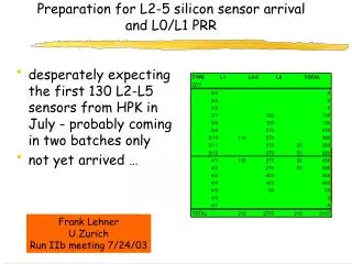
Update on Sensors • Sensor studies completed • Electrical characteristics of prototype L1 sensors and test structures • Irradiation studies reviewed and completed • Flux normalization verified via foil activation • Preparation for arrival of production sensors • Certification of sensor probing sites • Fermilab • Kansas State University • Stony Brook • Rochester (new probing site currently under development) • Visual and mechanical inspection prep • Procedures and database setup • Outer layer sensor order placed • 130 sensors arrived on 1 August 2003 • QA evaluation in progress
Advances in Other Areas • Second round SVX4 readout chip prototype approved, fabricated and currently under test • Yield appears to be high and chip appears fully functional • Hybrid and module burn-in test stands completed • Prototype analog cables delivered and tested • Prototype L0 hybrids delivered and tested • Grounding scheme on hybrids revised • Grounding scheme for inner layer support structures developed and being prototyped • Fabrication fixtures prototyped and tested • Mechanical grade pre-production stave fabricated • Electrical grade pre-production stave in progress • Carbon fiber (and autoclave) for stave shells ordered • Bearings placed on z=0 prototype bulkhead
Sensor Production Schedule • Hamamatsu provided a sensor production schedule which includes L0 and L1 sensors • Delivery of first batch of L2-5 sensors was almost on schedule
Sensor Delivery • If delivery of L0 sensors is completed • after 14 Sept 04, project misses DOE milestone • by 14 Sept 04 should not cause module production slip • If Hamamatsu L0 sensor production schedule just slips with the order date slip, then this order should be placed within 3 months to avoid module production slip • Order for L2-L5 sensors took six weeks from PRR to release • And, we have no prototype Hamamatsu L0 sensors, and would prefer to get a few asap for studies • after 16 Sept 04 puts L0 sensors on critical path • 2 days slack relative to current silicon ready to move date • If delivery of L1 sensors is completed • after 28 June 04, project misses DOE milestone • by 24 June 04 should not cause module production slip • If Hamamatsu L1 sensor production schedule just slips with order date slip, then this order should be placed within a month to avoid module production slip • after 4 October 04 puts L1 sensors on critical path • 14.2 weeks slack relative to current silicon ready to move date
Summary • Excellent progress on prototyping and pre-production of the D0 Run IIb Silicon Upgrade • Prototypes of all components of the design are in hand • Pre-production for most parts in progress • Remaining technical challenges are being addressed • Have started placing production orders • A strong, knowledgeable, experienced and very dedicated team is working hard (in a rather challenging climate) to produce the upgraded silicon detector that D0 needs to significantly enhance its performance throughout Run IIb • The constraints on the project dictate that we continue to push ahead in spite of the uncertainty
Charge • The Committee is requested to review the overall readiness for placing the production order for the inner layer sensors for the DZero Run IIb silicon detector. In particular, the project is requesting that the Committee evaluate the following items: • Whether the sensor specifications meet the technical requirements for Run IIb, recommending any changes that may be necessary. This should include, but not be limited to, consideration of results from radiation testing. • The completeness and viability of the quality assurance program the project has in place to qualify the production-version inner layer sensors, including a review of: • Soundness of the logistics of the testing and qualification plans; • Technical specifications and criteria for quality assurance; • Adequacy of the resources, both labor and equipment, that have been requested in the project plan for testing and QA. Included here should be an evaluation as to whether the throughput of qualified sensors will be adequate to maintain the project schedule; • The adequacy of the plans for logging data from sensor testing. • The overall technical readiness for placing the order, and the procurement readiness and strategy. If the Committee has any reservations here, it is requested that they describe what additional work should be done in order to meet proper readiness criteria.
Inner Layer Sensor PRR • Thank you for the insights, constructive comments, and recommendations that resulted from your review of the Outer Layer Sensors • Thanks for taking the time to help us in this important endeavor