Download
1 / 23
230 likes | 332 Views
PRR on Patch-Panel ASIC 9 Dec. 2002 KEK SOS. Overview LVDS Rx Variable Delay BCID Test Pulse Generator Control Radiation tests Mass-production and inspection. Overview. Requirements Receives LVDS differential signals from two ASD Boards (2 x 16-ch) BCID

E N D
PRR on Patch-Panel ASIC9 Dec. 2002 KEK SOS • Overview • LVDS Rx • Variable Delay • BCID • Test Pulse Generator • Control • Radiation tests • Mass-production and inspection
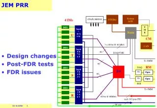
Overview • Requirements • Receives LVDS differential signals from two ASD Boards (2 x 16-ch) • BCID • Variable delays (common for 16-ch signals from a ASD Board) for phase adjustment, variable delays for the clock • Effectively wider gate width than 25 nsec • Variable delays • 25 nsec dynamic range with a step of sub-nano sec. • Two Test Pulse Generators for two ASD Boards with variable amplitude and variable delay • JTAG Control • Process • 0.35 mm full-custom CMOS (Rohm)
LVDS Receiver (I) • Propagation delay vs. amplitude and offset voltage
LVDS Receiver (II) • Dependence on supply voltage
Control via JTAG • BYPASS, No Boundary Scan • TRST_ is not supported. • BCID (Port-A and Port-B) • Mask, Signal Delay, BCID CLK Delay, Gate Width • Test Pulse (Port-A and Port-B) • Amplitude, Fine Delay, Coarse Delay • Debug Variable Delay • SEU flag
Control via input pins • POL • Set whether anode or cathode signals • PLL • ENB, ENV, ENP, SELECT_ENP (test purpose) • STEP0, 1:The number of Delay Units in PLL • STEP decides the dynamic range and a step of the Variable Delay • BCID skip (BYPASS) • Test Pulse Trigger (TPTRG) • RESET_ • Reset all the register to the defaults. • Initiate PLL lock sequence
Radiation Environment (Patch-Panel ASIC) • TID RTC=10.5 krad • SFsim=3.5, SFldr=5, SFlot=2 • RTC=0.3 (Gray/y) x 3.5 x 5 x 2 x 10 years = 105 Gray • Simulated Radiation Level (SRL) for SEE • SRL = 2.11 x 10¹⁰ h/cm2/10years • Rohm 0.35mm CMOS Process • The same process with SLB ASIC • We can deduce the radiation effect from the result of SLB ASICs. • The voting logic is used to all the instruction and data registers.
Radiation Test (TID) • Research Center for Nuclear Science and Technology (RCNST) in Univ. of Tokyo (26 Nov. 02) • 60Co, 0.954 krad/min., 4 samples • 30, 30, 30 and 85 krad • Biased during irradiation • Current measurement • The increase of the current can be observed at more than 30 krad. • Functionality checks before/after irradiation • No functional defect was observed in all 4 chips.
Radiation Test (SEE) • AVF Cyclotron at CYRIC of Tohoku Univ. • Proton beam: E=70 MeV, I=2-4 nA • Beam Fluence and profile using dosimetry • 0.1mm thick Cu foil put on the DUT • Gamma-ray spectra from activated radioisotopes will be measured using a Ge detector. • Intensity distribution of the g-ray will be measured with an Imaging Plate. • 4 ASICs will be tested. • Beam time is 17-18 Dec. (48 hours)
Mass-Production • 10,368 + spares = 15,000 working chips • The re-production of the mask will dominate the price. • Combine the mask and mass-production with other ASICs • JRC ASIC (5 mm x 5 mm, 1600 chips) • SLB ASIC (10 mm x 10 mm, 3000 chips) • Rohm has started their consideration how to proceed the mass-productions. • International Tendering in summer 2003 • Completion of the mass-production by the end of 2003
Inspection • At IC production line (Rohm) • Need negotiations, but they are hesitating. • DC parameters (DC currents) • At KEK • AC measurements • PPGs, FIFO Modules and PT4 modules in VME • Development of a Test Board and software • Comprehensive tests should be done as a PS-Board • 2 [person X month] • Manpower for inspection