Download
1 / 28
470 likes | 1.55k Views
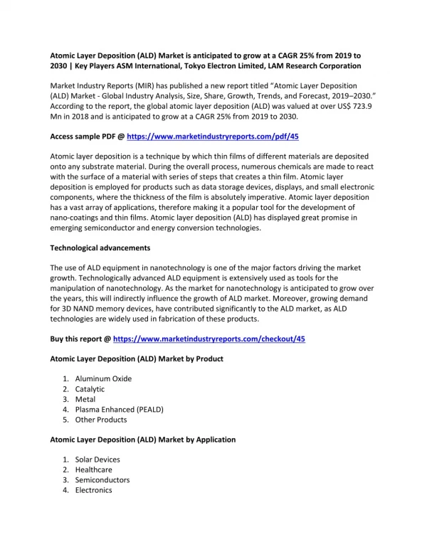
Atomic Layer Deposition (ALD). Presented by Myo Min Thein EE 518 Class Presentation, Penn State Spring 2006 Instructor: Dr. J. Ruzyllo. Presentation Overview. Definition of ALD Brief history of ALD ALD process and equipments ALD applications Summary. Definition of ALD.

E N D
Atomic Layer Deposition (ALD) Presented by Myo Min Thein EE 518 Class Presentation, Penn State Spring 2006 Instructor: Dr. J. Ruzyllo
Presentation Overview • Definition of ALD • Brief history of ALD • ALD process and equipments • ALD applications • Summary EE 518 Class Presentation
Definition of ALD • ALD is a method of applying thin films to various substrates with atomic scale precision. • Similar in chemistry to chemical vapor deposition (CVD), except that the ALD reaction breaks the CVD reaction into two half-reactions, keeping the precursor materials separate during the reaction. • ALD film growth is self-limited and based on surface reactions, which makes achieving atomic scale deposition control possible. • By keeping the precursors separate throughout the coating process, atomic layer thickness control of film grown can be obtained as fine as atomic/molecular scale per monolayer. Ref: "Atomic Layer Deposition," Wikipedia: The Free Encyclopedia, Wikimedia Foundation, 24 April 06. <http://en.wikipedia.org/wiki/Atomic_Layer_Deposition>. EE 518 Class Presentation
Definition of ALD • ALD is a method of applying thin films to various substrates with atomic scale precision. • Similar in chemistry to CVD, except that the ALD reaction breaks the CVD reaction into two half-reactions, keeping the precursor materials separate during the reaction. • ALD film growth is self-limited and based on surface reactions, which makes achieving atomic scale deposition control possible. • By keeping the precursors separate throughout the coating process, atomic layer thickness control of film grown can be obtained as fine as atomic/molecular scale per monolayer. Ref: "Atomic Layer Deposition," Wikipedia: The Free Encyclopedia, Wikimedia Foundation, 24 April 06. <http://en.wikipedia.org/wiki/Atomic_Layer_Deposition>. EE 518 Class Presentation
Definition of ALD • ALD is a method of applying thin films to various substrates with atomic scale precision. • Similar in chemistry to chemical vapor deposition (CVD), except that the ALD reaction breaks the CVD reaction into two half-reactions, keeping the precursor materials separate during the reaction. • ALD film growth is self-limited and based on surface reactions, which makes achieving atomic scale deposition control possible. • By keeping the precursors separate throughout the coating process, atomic layer thickness control of film grown can be obtained as fine as atomic/molecular scale per monolayer. Ref: "Atomic Layer Deposition," Wikipedia: The Free Encyclopedia, Wikimedia Foundation, 24 April 06. <http://en.wikipedia.org/wiki/Atomic_Layer_Deposition>. EE 518 Class Presentation
Definition of ALD • ALD is a method of applying thin films to various substrates with atomic scale precision. • Similar in chemistry to chemical vapor deposition (CVD), except that the ALD reaction breaks the CVD reaction into two half-reactions, keeping the precursor materials separate during the reaction. • ALD film growth is self-limited and based on surface reactions, which makes achieving atomic scale deposition control possible. • By keeping the precursors separate throughout the coating process, atomic layer thickness control of film grown can be obtained as fine as atomic/molecular scale per monolayer. Ref: "Atomic Layer Deposition," Wikipedia: The Free Encyclopedia, Wikimedia Foundation, 24 April 06. <http://en.wikipedia.org/wiki/Atomic_Layer_Deposition>. EE 518 Class Presentation
Brief History of ALD • Introduced in 1974 by Dr. Tuomo Suntola and co-workers in Finland to improve the quality of ZnS films used in electroluminescent displays. • Recently, it turned out that ALD also produces outstanding dielectric layers and attracts semiconductor industries for making High-K dielectric materials. Ref: "History of Atomic Layer Deposition (ALD)," Finnish MicroNanoTechnology Network (FMNT), 24 April 2006. <http://www.fmnt.fi/index.pl?id=2913&isa=Category&op=show>. EE 518 Class Presentation
Brief History of ALD • Introduced in 1974 by Dr. Tuomo Suntola and co-workers in Finland to improve the quality of ZnS films used in electroluminescent displays. • Recently, it turned out that ALD method also produces outstanding dielectric layers and attracted semiconductor industries for making High-K dielectric materials. Ref: "History of Atomic Layer Deposition (ALD)," Finnish MicroNanoTechnology Network (FMNT), 24 April 2006. <http://www.fmnt.fi/index.pl?id=2913&isa=Category&op=show>. EE 518 Class Presentation
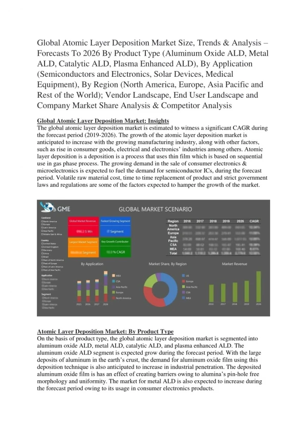
ALD Process and Equipments • Releases sequential precursor gas pulses to deposit a film one layer at a time on the substrate. • The precursor gas is introduced into the process chamber and produces a monolayer of gas on the wafer surface. A second precursor of gas is then introduced into the chamber reacting with the first precursor to produce a monolayer of film on the wafer surface. Two fundamental mechanisms: • Chemisorption saturation process • Sequential surface chemical reaction process • Example: ALD cycle for Al2O3 deposition • Since each pair of gas pulses (one cycle) produces exactly one monolayer of film, the thickness of the resulting film may be precisely controlled by the number of deposition cycles. Ref: A. Knop–Gericke, "Preparation of Model Systems by Physical Methods," a lecture given at Modern Methods in Heterogeneous Catalysis Research Lecture Series, Fritz Haber Institute of the Max Planck Society. 24 April 06. <http://w3.rz-berlin.mpg.de/%7Ejentoft/lehre/catalysis0405.html>. EE 518 Class Presentation
ALD Process and Equipments • Releases sequential precursor gas pulses to deposit a film one layer at a time. • A first precursor gas is introduced into the process chamber and produces a monolayer of gas on the wafer surface. Then a second precursor of gas is introduced into the chamber reacting with the first precursor to produce a monolayer of film on the wafer surface. Two fundamental mechanisms: • Chemisorption saturation process • Sequential surface chemical reaction process • Example: ALD cycle for Al2O3 deposition • Since each pair of gas pulses (one cycle) produces exactly one monolayer of film, the thickness of the resulting film may be precisely controlled by the number of deposition cycles. Ref: A. Knop–Gericke, "Preparation of Model Systems by Physical Methods," a lecture given at Modern Methods in Heterogeneous Catalysis Research Lecture Series, Fritz Haber Institute of the Max Planck Society. 24 April 06. <http://w3.rz-berlin.mpg.de/%7Ejentoft/lehre/catalysis0405.html>. EE 518 Class Presentation
ALD Process and Equipments • Releases sequential precursor gas pulses to deposit a film one layer at a time. • A first precursor gas is introduced into the process chamber and produces a monolayer of gas on the wafer surface. Then a second precursor of gas is introduced into the chamber reacting with the first precursor to produce a monolayer of film on the wafer surface. Two fundamental mechanisms: • Chemisorption saturation process • Sequential surface chemical reaction process • Example: ALD cycle for Al2O3 deposition (Step 1a) Ref: "Atomic Layer Deposition," Cambridge NanoTech Inc., 24 April 06. <http://www.cambridgenanotech.com/>. EE 518 Class Presentation
ALD Process and Equipments • Releases sequential precursor gas pulses to deposit a film one layer at a time. • A first precursor gas is introduced into the process chamber and produces a monolayer of gas on the wafer surface. Then a second precursor of gas is introduced into the chamber reacting with the first precursor to produce a monolayer of film on the wafer surface. Two fundamental mechanisms: • Chemisorption saturation process • Sequential surface chemical reaction process • Example: ALD cycle for Al2O3 deposition (Step 1b) Ref: "Atomic Layer Deposition," Cambridge NanoTech Inc., 24 April 06. <http://www.cambridgenanotech.com/>. EE 518 Class Presentation
ALD Process and Equipments • Releases sequential precursor gas pulses to deposit a film one layer at a time. • A first precursor gas is introduced into the process chamber and produces a monolayer of gas on the wafer surface. Then a second precursor of gas is introduced into the chamber reacting with the first precursor to produce a monolayer of film on the wafer surface. Two fundamental mechanisms: • Chemisorption saturation process • Sequential surface chemical reaction process • Example: ALD cycle for Al2O3 deposition (Step 1c) Ref: "Atomic Layer Deposition," Cambridge NanoTech Inc., 24 April 06. <http://www.cambridgenanotech.com/>. EE 518 Class Presentation
ALD Process and Equipments • Releases sequential precursor gas pulses to deposit a film one layer at a time. • A first precursor gas is introduced into the process chamber and produces a monolayer of gas on the wafer surface. Then a second precursor of gas is introduced into the chamber reacting with the first precursor to produce a monolayer of film on the wafer surface. Two fundamental mechanisms: • Chemisorption saturation process • Sequential surface chemical reaction process • Example: ALD cycle for Al2O3 deposition (Step 2a) Ref: "Atomic Layer Deposition," Cambridge NanoTech Inc., 24 April 06. <http://www.cambridgenanotech.com/>. EE 518 Class Presentation
ALD Process and Equipments • Releases sequential precursor gas pulses to deposit a film one layer at a time. • A first precursor gas is introduced into the process chamber and produces a monolayer of gas on the wafer surface. Then a second precursor of gas is introduced into the chamber reacting with the first precursor to produce a monolayer of film on the wafer surface. Two fundamental mechanisms: • Chemisorption saturation process • Sequential surface chemical reaction process • Example: ALD cycle for Al2O3 deposition (Step 2b) Ref: "Atomic Layer Deposition," Cambridge NanoTech Inc., 24 April 06. <http://www.cambridgenanotech.com/>. EE 518 Class Presentation
ALD Process and Equipments • Releases sequential precursor gas pulses to deposit a film one layer at a time. • A first precursor gas is introduced into the process chamber and produces a monolayer of gas on the wafer surface. Then a second precursor of gas is introduced into the chamber reacting with the first precursor to produce a monolayer of film on the wafer surface. Two fundamental mechanisms: • Chemisorption saturation process • Sequential surface chemical reaction process • Example: ALD cycle for Al2O3 deposition (Step 2c) Ref: "Atomic Layer Deposition," Cambridge NanoTech Inc., 24 April 06. <http://www.cambridgenanotech.com/>. EE 518 Class Presentation
ALD Process and Equipments • Releases sequential precursor gas pulses to deposit a film one layer at a time. • A first precursor gas is introduced into the process chamber and produces a monolayer of gas on the wafer surface. Then a second precursor of gas is introduced into the chamber reacting with the first precursor to produce a monolayer of film on the wafer surface. Two fundamental mechanisms: • Chemisorption saturation process • Sequential surface chemical reaction process • Example: ALD cycle for Al2O3 deposition (after 3 cycles) Ref: "Atomic Layer Deposition," Cambridge NanoTech Inc., 24 April 06. <http://www.cambridgenanotech.com/>. EE 518 Class Presentation
ALD Process and Equipments • Releases sequential precursor gas pulses to deposit a film one layer at a time. • A first precursor gas is introduced into the process chamber and produces a monolayer of gas on the wafer surface. Then a second precursor of gas is introduced into the chamber reacting with the first precursor to produce a monolayer of film on the wafer surface. Two fundamental mechanisms: • Chemisorption saturation process • Sequential surface chemical reaction process • Example: ALD cycle for Al2O3 deposition • Since each pair of gas pulses (one cycle) produces exactly one monolayer of film, the thickness of the resulting film may be precisely controlled by the number of deposition cycles. Step coverage and deposition rate Vs. deposition technique. Ref: "Technology Backgrounder: Atomic Layer Deposition," IC Knowledge LLC, 24 April 06. <www.icknowledge.com/misc_technology/Atomic%20Layer%20Deposition%20Briefing.pdf>. EE 518 Class Presentation
ALD Process and Equipments Four main types of ALD reactors • Closed system chambers • Open system chambers • Semi-closed system chambers • Semi-open system chambers EE 518 Class Presentation
ALD Process and Equipments Four main types of ALD reactors • Closed system chambers (most common) • Open system chambers • Semi-closed system chambers • Semi-open system chambers EE 518 Class Presentation
Schematic of a closed ALD system ALD Process and Equipments Four main types of ALD reactors • Closed system chambers (most common) • The reaction chamber walls are designed to effect the transport of the precursors. • Open system chambers • Semi-closed system chambers • Semi-open system chambers Ref: "Technology Backgrounder: Atomic Layer Deposition," IC Knowledge LLC, 24 April 06. <www.icknowledge.com/misc_technology/Atomic%20Layer%20Deposition%20Briefing.pdf>. EE 518 Class Presentation
The Verano 5500™ A 300-mm ALD system by Aviza Technology, Inc [2]. ALD Process and Equipments [1] [1] Process Temperature [1] 1 "Technology Backgrounder: Atomic Layer Deposition," IC Knowledge LLC, 24 April 06. <www.icknowledge.com/misc_technology/Atomic%20Layer%20Deposition%20Briefing.pdf> 2 ”Atomic Layer Deposition," Aviza Technology. 26 April 06. <http://www.avizatechnology.com/products/verano.shtml>. EE 518 Class Presentation
The Verano 5500™ A 300-mm ALD system by Aviza Technology, Inc [2]. ALD Process and Equipments One cycle [1] [1] Acceptable temperature range for deposition. Process Temperature [1] 1 "Technology Backgrounder: Atomic Layer Deposition," IC Knowledge LLC, 24 April 06. <www.icknowledge.com/misc_technology/Atomic%20Layer%20Deposition%20Briefing.pdf>. 2 ”Atomic Layer Deposition," Aviza Technology. 26 April 06. <http://www.avizatechnology.com/products/verano.shtml>. EE 518 Class Presentation
ALD Applications • High-K dielectrics for CMOS • Semiconductor memory (DRAM) • Cu interconnect barrier • Deposition in porous structures EE 518 Class Presentation
ALD Applications • High-K dielectrics for CMOS • Semiconductor memory (DRAM) • Cu interconnect barrier • Deposition in porous structures EE 518 Class Presentation
Reduces leakage current • Faster switching speed • Cooler transistors ALD Applications • High-K dielectrics for CMOS Candidates for High-K dielectrics FilmPrecursors Al2O3 Al(CH)3, H2O or O3 HfO2 HfCl4 or TEMAH, H2O ZrO2 ZrCl4, H2O Ref: "Intel's High-k/Metal Gate Announcement," Intel® Corporation. 26 April, 06. <http://www.intel.com/technology/silicon/micron.htm#high>. EE 518 Class Presentation
All these applications take advantage of uniformity, conformal step coverage, precise thickness control of deposited films, which can be achieved by ALD deposition method. ALD Applications • High-K dielectrics for CMOS • Semiconductor memory (DRAM) • Cu interconnect barrier • Deposition in porous structures Step coverage and deposition rate Vs. deposition technique. Ref: "Technology Backgrounder: Atomic Layer Deposition," IC Knowledge LLC, 24 April 06. <www.icknowledge.com/misc_technology/Atomic%20Layer%20Deposition%20Briefing.pdf>. EE 518 Class Presentation
Summary • Advantages • Stoichiometric films with large area uniformity and 3D conformality. • Precise thickness control. • Low temperature deposition possible. • Gentle deposition process for sensitive substrates. • Disadvantages • Deposition Rate slower than CVD. • Number of different material that can be deposited is fair compared to MBE. EE 518 Class Presentation