Download
1 / 5
50 likes | 267 Views
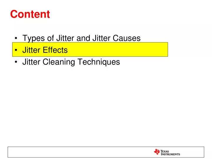
Content. Types of Jitter and Jitter Causes Jitter Effects Jitter Cleaning Techniques. Jitter Effects Clocking Data Converters (1). ADC. f3 = 3*f2. V in (volts). Clock Generator. Distribution of the sampled voltage value due to sampling jitter. . f2 = X.

E N D
Content • Types of Jitter and Jitter Causes • Jitter Effects • Jitter Cleaning Techniques
Jitter EffectsClocking Data Converters (1) ADC f3 = 3*f2 Vin (volts) Clock Generator Distribution of the sampled voltage value due to sampling jitter. f2 = X • Sampling jitter has two components: • Jitter on the sampling clock • Aperture jitter from the ADC. • Because they are uncorrelated, these jitters are combined as the root sum square: f1 = DC time (s) Tsample- s tsample Tsample+ s
Jitter EffectsClocking Data Converters (2) Assuming a sinusoidal input for Vin we have, Differentiating with respect to time yields the signal slope, RMS Taking the RMS value, Therefore, the RMS error voltage due to jitter is Therefore, the SNR component due to jitter is: Signal to noise ratio (SNR) is defined by,
Jitter EffectsClocking Data Converters (4) Signal path with effective resolution of 12-bit and an input bandwidth of 500MHz requires a clock with less than 200 fs of total jitter!