Download
1 / 62
760 likes | 1.1k Views
Understanding Operational Amplifier Limitations and Long-Term Stability. By Marek Lis Sr Application Engineer Texas Instruments -Tucson. Introductions. Art Kay, PA-Linear Applications Manager Mixed Signal “System-on-a-Chip” Bridge Sensor Signal Conditioning

E N D
Understanding Operational Amplifier Limitations and Long-Term Stability By Marek Lis Sr Application Engineer Texas Instruments -Tucson
Introductions • Art Kay, PA-Linear Applications Manager • Mixed Signal “System-on-a-Chip” • Bridge Sensor Signal Conditioning • Evaluation Modules (hardware / software) • Noise • Northrop Grumman, Burr-Brown (Test Engineering) • Cleveland State, Georgia Tech Grad.
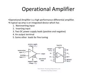
Summary of Topics • Review of Op-Amp Input Topologies • Common Mode limits • Causes of Op-Amp Output Phase Inversion • Bipolar vs. JFET input effects caused by exceeding the Vcm • Review of Op-Amp Output Topologies • Output Swing limits • Long-Term Stability Spec • for specs centered around a fixed value • for parameters specified as an absolute value
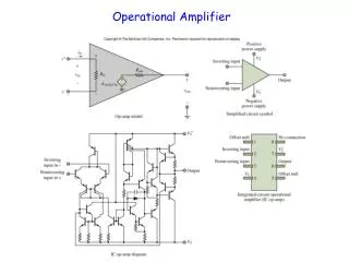
Input Stage Considerations
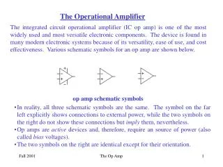
OP AMP OPERATION vs SUPPLY VOLTAGE Each amplifier has 36V supplies! The common mode in each case is the supply midpoint. All amps can act as “single supply” Note: A single-supply optimized op amp is not the same as a single supply op amp.
Simplified schematic of OPA336 input stage(Swing to Positive Rail)
Simplified schematic of OPA336 input stage (Swing to Negative Rail)
Simplified schematic of OPA827 input stageSwing to Negative Rail
Remember from Earler in the presentation… The limit is based on the positive supply minus saturation voltage and Vgs.
MOSFET Charge Pump (rail-to-rail) • Supplies a small current to input • GBW = 50MHz, Charge Pump Freq=10MHz
MOSFET Zero Drift (rail-to-rail) No Offset Correction With Offset Correction
Chopper topology Minor aliasing issue Best noise Low freq. Wide band Ripple Issue (frequency close to UGB) Auto-zero topology Aliasing issue Increased noise Low freq. Wide band Low ripple (low frequency ~ few kHz) Topology Summary
Op Amp Output Phase Inversion
PNP Bipolar Input Op Amp Low Common-Mode LimitationNormal Operation – No Phase Inversion
PNP Bipolar Input Op Amp Low Common-Mode LimitationPhase Inversion Issue!
Summary of Output Phase Inversion What causes a phase reversal? Exceeding the input common-mode voltage range may cause a phase reversal. How can it be prevented? Staying with op amp specified Vcm linear region Using op amp with a built-in anti-phase reversal circuitry Utilizing external circuitry to prevent a phase inversion Is it process dependent? Some built-in anti-phase reversal circuitry might be process dependent depending on topology used Most modern op amps use a robust topologies assuring no phase reversal How can a customer be confidant of no phase reversal? (if it is not explicitly stated in the data sheet) Apply a slow triangular waveform in a buffer configuration 1V beyond rails to test for phase inversion - you must limit the input current to less than 10mA to prevent damaging IC
Output Stage Considerations
Classic Output Stage • Common-emitter output • Current source driver • Headroom set by VBE+VCESAT • Unity Gain VBE VBE
OPA827 – Classic Output OPA827 OPA827 Short Circuit Limit Output Saturated
OPA827 – Classic Output OPA827 The Table Output Swing is defined at: Vout swing = 18V – 3V = ±15V Iout = 15V/1k = 15mA For Aol > 120dB As you approach the limit or increase ILOAD, Aol will decrease.
R-to-R Output Stage Vsat = 50mV to ≈ 1mV Vsat = 0.2V • Common Collector or Common Drain • Headroom set by VDSsat or VCEsat • On bipolar sat is approximately 0.2V • After sat Beta drops dramatically • On FET sat is limited by output transistor scaling • Can achieve very low sat values (e.g. mV)
R-to-R Output Stage • Value of RLOAD affects AOL and Output Swing • the gain in the last stage is set by rout / gm • rout decreases with loading
Why can’t we get Rail-to-Rail on CMOS?MOSFET Characteristic Curves • Some minimum drain to source voltage is required. • Increasing current requires more Vgs.
OPA211 – rail-to-rail Out (Bipolar) Loading limits output swing and reduces Aol.
SS Pull Down Cheat Sheet Selected to sink quiescent current in output stage. Approximately ½ Iq.
Gaussian (or Normal) Distribution 68% within ±1 standard deviation 99.7% within ±3 standard deviations
Double Ended Limit Symmetrical Limits: Max = 150uV is +/-150uV Mean = often approximately zero Typical = Mean + σ ≈ σ Max = + 3σ (or greater) Min = - 3σ (or smaller)
Long-Term (10 year) Shift for Gaussian Distributions(Centered around a Mean Value) Initial PDS Distribution (blue) vs Long-Term Parametric Shift (green) For 10 year life of a product.
Life-Time Vos and Vos Temp Drift Shift Max LT Vos = 240uV Max LT Vos Drift = 2.0uV/C Life-Time Max Shift (ten-year) = Max Initial Value Long-Term Max Spec = 2 * Initial Spec
Life-Time Output Voltage Initial Accuracy Shift(specs centered around a fixed value) Max LT Vref = +/-0.1%