Download
1 / 60
890 likes | 1.25k Views
Operational Amplifier. 1.0 Operational Amplifier. 1.1 Introduction 1.2 Ideal Op-Amp 1.3 Op-amp input modes 1.4 Op-amp Parameters 1.5 Operation Single-mode Differential-mode Common-mode operation 1.6 Op-Amps basics 1.7 Datasheet. 1.1 Introduction. Typical IC packages.

E N D
1.0 Operational Amplifier • 1.1 Introduction • 1.2 Ideal Op-Amp • 1.3 Op-amp input modes • 1.4 Op-amp Parameters • 1.5 Operation • Single-mode • Differential-mode • Common-mode operation • 1.6 Op-Amps basics • 1.7 Datasheet
1.1 Introduction Typical IC packages IC packages placed on circuit board
Uses of Op-Amp • To provide voltage amplitude changes (amplitude and polarity) • Comparators • Oscillators • Filter circuits • Instrumentation circuits
Op-Amp Basics Basic Op-amp Note: Terminals for dc supply are omitted
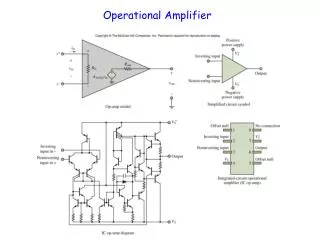
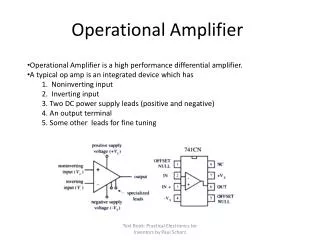
Definition • The operational amplifier (op-amp) is a circuit of components integrated into one chip. • Op-amps were used to model the basic mathematical operations: addition, subtraction, integration, differentiation, and etc in electronic analog computers. • A typical op-amp is powered by two dc voltages (+V and –V) and has an inverting (-) and a non-inverting input (+) and an output.
Op-amp schematic symbol • Two dc Supply voltages • +V : Positive • -V : Negative • One Output Terminal • Two Input Terminal • Inverting (-) input • Non-inverting (+) input
1.2 Ideal / Practical Op-Amp Ideal Op-Amp • voltage gain (Av) = ∞ • bandwidth = ∞ • input impedance (Zin) = ∞ • output impedance (Zout) = 0
Practical Op-Amp • Voltage gain (Av) very ↑. • Input impedance (Zin) very ↑. • Output impedance (Zout) very ↓.
Properties Ideal Op-Amp Practical Op-Amp • Infinite input impedance • Zero output impedance • Infinite open-loop gain • Infinite bandwidth • Zero noise contribution • Zero DC output offset • Both differential inputs stick together • input impedance 500k-2M • output impedance 20-100 • open-loop gain (20k to 200k) • Bandwidth limited (a few kHz) • noise contribution • Non-zero DC output offset
Input Impedance (Zin) • Input impedance (Zin) is measured across the input terminals. • It is the Thevenin resistance of the internal connection between the two input terminals. • Input impedance (Zin) is the ratio of input voltage (Vin) to input current (Iin).
When Zin = ∞, the input current (Iin) = 0. • So, any current will neither flowing from the source supply into the amplifiers input circuitry, nor will accept current from any external circuit. • In real, the resistance is 500k to 2M.
Output Impedance (Zout) • The internal resistance of the op-amp is op-amp output impedance, Zout. • This internal resistance is in series with the load, reducing the output voltage available to the load. • The output impedance of the ideal operational amplifier is assumed to be zero acting as a perfect internal voltage source with no internal resistance, so that it can supply as much current as necessary to the load. • Real op-amps have output impedance in the range 20-100 .
Open-Loop Gain (A0l) • Open-Loop Gain, Aol is the gain of the op-amp without feedback. • In the ideal op-amp, Aol is infinite. • In real op-amp is (20k to 200k).
Bandwidth (BW) • The ideal op-amp will amplify all signals from DC to the highest AC frequencies. • In real op-amps, the bandwidth is rather limited. • This limitation is specified by the Gain-Bandwidth product, which is equal to the frequency where the amplifier gain becomes unity. • Some op-amps, such as 741 family, have very limited bandwidth up to a few kHz.
Noise Contribution • In an ideal op amp, all noise voltages produced are external to the op-amp. • Thus any noise in the output signal must have been in the input signal as well. • The ideal op amp contributes nothing extra to the output noise.
Output Offset Voltage • The output offset voltage of any amplifier is the output voltage that exists when it should be zero. • The voltage amplifier sees zero input voltage when both inputs are grounded. This connection should produce a zero output voltage. • If the output is not zero then there is said to be an output voltage present. • In the ideal op amp this offset voltage is zero volts. • In practical op amps the output offset voltage is nonzero.
Both Differential Inputs Stick Together • This means that a voltage applied to one inverting inputs also appears at the other non-inverting inputs. • If we apply a voltage to the inverting input (-) and then connect a voltmeter between the non-inverting input (+) and the power supply common, then the voltmeter will read the same potential on non-inverting as on the inverting input.
1.3 Op-Amp Input Modes Single-Ended Differential Mode Input input signal is connected to one input and the other input is grounded. Two possible configuration: • Inverting () terminal is grounded and input signal is applied to the non-inverting (+) terminal. In this configuration, the resultant output signal is in phase with the input signal.
2. The non-inverting (+) terminal is grounded and input signal is applied to the inverting () terminal. In this configuration, the resultant output signal is in anti-phase with the input signal.
Double-Ended Differential Mode Input • Two out-of-phase (opposite-polarity) signals are applied to the inputs. • The amplified difference between the two inputs appears on the output.
Common Mode Input • Two signals of same phase, frequency, and amplitude are applied to the inputs which results in Vout = 0 (signals cancel). (Practically, a small output signal will result.) • This is called common-mode rejection. This type of mode is used to remove unwanted noise signals and do not distort the desired signal.
1.4 Op-Amp Parameters Common-Mode Rejection Ratio (CMRR) • The ability of amplifier to reject the common-mode signals (noise). • Ratio of open-loop gain (Aol) to common-mode gain (Acm): • The higher the CMRR, the better. • open-loop gain (Aol) is high and common-mode gain (Acm) is low.
CMRR = 100,000 means that the desired input signal (differential) is amplified 100,000 times more than the unwanted noise (common-mode). • If the amplitudes of the differential input signal and the common-mode noise are equal, the desired signal will appear on the output 100,000 times greater in amplitude than the noise. • Thus, the noise has been essentially eliminated.
Common-Mode Input Voltage • The range of input voltages which, when applied to both inputs, will not cause clipping or other output distortion. Input Offset Voltage (VOS) • The differential dc voltage required between the inputs to force the output to zero volts (0V). • Typical VOS are in the range of 2 mV or less.
Input Bias Current (IBIAS) • Is the average of the two dc currents required to bias the differential amplifier. • Is the average of both input currents.
Input Offset Current (IOS) • The difference in the input bias currents:
Offset Voltage error
Input Impedance (ZIN) 1. Differential input impedance (ZIN(d)) is the total resistance between the inverting and non-inverting inputs. • Differential impedance is measured by the changes of differential input voltage over changes of bias current:
2. Common-mode input impedance (ZIN(cm)) is the resistance between each input and ground. • Common-mode input impedance is measured by the changes of common-mode input voltage over changes of bias current.
Output Impedance (Zout) • The resistance viewed from the output terminal of the op-amp.
Slew Rate • The maximum rate of change in the output voltage per unit of time.
Example 1 The output voltage of a certain op-amp appears as figure below in response to a step input. Determine the slew rate.
Negative Feedback In Op-Amp Circuits • Negative feedback is feeding part of the output back to the input to limit the overall gain. • This is used to make the gain more realistic so that the op-amp is not driven into saturation. Remember that regardless of gain, there are limitations of the amount of voltage that an amplifier can produce. • with –ve feedback closed loop gain can be reduced and controlled so that op-amp can function as a linear amplifier. Without negative feedback
Op-Amps With Negative Feedback • The extremely high open-loop gain of an op-amp creates an unstable because a small noise voltage on the input can be amplified to a point where the amplifier is driven out of its linear region. • With negative feedback, the gain can be stabilize and the frequency response can be increased. • Negative feedback takes a portion of the output and applies it back out of phase with the input, creating an effective reduction in gain. • The closed loop gain is much less than the open loop gain and independent of it.
Op-Amps With Negative Feedback Noninverting Amplifier • The closed-loop voltage gain (Acl) is the voltage gain of an op-amp with external feedback. • The gain can be controlled by external component values.
Op-Amps With Negative Feedback • The voltage-follower amplifier configuration has all of the output signal fed back to the inverting input. • The voltage gain is 1. • This makes it useful as a buffer amp since it has a high input impedance and low output impedance.
Op-Amps With Negative Feedback: Inverting • The inverting amplifier has the output fed back to the inverting input for gain control. • The gain for the inverting op-amp can be determined by the formula below. A cl(I) = - Rf /Ri
Effects Of Negative Feedback On Op-Amp Impedances Input Impedance Noninverting However high the input impedance of an op-amp circuit is, impedance still exists. For a noninverting amplifier it can be determined by the formulas below. B(feedback attenuation) = Ri/(Ri + Rf) Zin(NI) = (1 + AolB)Zin
Effects Of Negative Feedback On Op-Amp Impedances Output Impedance The output impedance is understood to be low for an op-amp. Its exact value can be determined by the formula below. Z(out)(NI) = Zout/1 + AolB Noninverting
Effects Of Negative Feedback On Op-Amp Impedances The input impedance for an inverting amplifier is approximately equal to the input resistor (Ri). Zin(I) Ri The output impedance is very low and in most cases any impedance load can be connected to it with no problem. The exact amount can be determined by the formulas below. B(feedback attenuation) = Ri/Ri + Rf Zout(I) = Zout / (1 + AolB) Inverting
Voltage-Follower Impedances: • Voltage-follower is a special case of noninverting amplifier but with B = 1
Effect of an Input Bias Current. Input bias current creates output error voltage (I1Rf) in inverting amplifier. Input bias current creates output error voltage in a voltage-follower.
Input bias current creates output error voltage in noninverting amplifier. Effect of an Input Bias Current.
Bias Current Compensation in a Voltage-Follower Input bias current creates an output error voltage that must be compensated for in all of the op-amp configurations. For the voltage-follower this error voltage can be reduced with resistors of the same value in the feedback loop and input.
Bias Current Compensation For the inverting and noninverting configurations this can be accomplished by a resistor in the noninverting part of the circuit that has the same value as the feedback resistor.
Input Offset Voltage Compensation Input offset voltage is small but unavoidable because of internal characteristic differences. The offset null terminals and a potentiometer connected as shown can eliminate this.
Open-Loop Response Remember Op-Amp Gains?