Download
1 / 29
290 likes | 387 Views
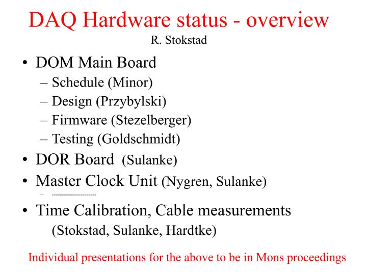
DAQ Hardware status - overview R. Stokstad. DOM Main Board Schedule (Minor) Design (Przybylski) Firmware (Stezelberger) Testing (Goldschmidt) DOR Board (Sulanke) Master Clock Unit (Nygren, Sulanke) ---------------------- Time Calibration, Cable measurements

E N D
DAQ Hardware status - overviewR. Stokstad • DOM Main Board • Schedule (Minor) • Design (Przybylski) • Firmware (Stezelberger) • Testing (Goldschmidt) • DOR Board (Sulanke) • Master Clock Unit (Nygren, Sulanke) • ---------------------- • Time Calibration, Cable measurements (Stokstad, Sulanke, Hardtke) Individual presentations for the above to be in Mons proceedings
Icecube DOM MB Status and Development Schedule • April – Oct '03 • Rev 2 test and development (22 boards) • Oct – Nov ’03 • Rev 3 fabrication and test (16 boards) • Nov ’03 – Mar ’04 • Rev 4 fabrication and test (60 boards) • March – June ’04 • Rev 5 for deployment (420 boards)
Rev 3 status • October – November ‘03 • First 4 cards due Oct 22, 12 more to follow 5 days after approval • Changes from Rev 2 address memory performance at temperature and signal quality issues • Testing at LBNL will include manual tests and STF testing • Temp cycling of bare and loaded boards • +65, -40degC 10 cycles • First 4 cards to UW, later to LBNL • 8 cards to UW, 8 cards to LBNL
Rev 4 plans • November – March ‘04 • Design modifications as indicated by Rev 3 tests and internal review • Final parts selection for reliability • 60 cards to be fabricated • “Qualification test” at UW • Longer term temperature tests • String operation tests • Some boards used for development at LBNL
Rev 5 plans • Initial production review November ‘03 • Based on Rev 3 and Rev 4 tests • Earlier than usual to allow long-lead parts purchasing • Production readiness review - January ‘04 • Based on initial Rev 4 tests • Qualification testing • Vendor qualifications • Fabrication process approval
Rev 5 Production (March – June ’04) • Full production and Q/A procedures in place • All parts as selected for reliability • ATWD production run including qualification tests • Any differences between Rev 4 and Rev 5 require formal Engineering Change Procedure and re-qualification testing • Fabrication begins March ‘04 • Testing begins April ’04 • Delivery April - June ‘04
Some Changes made in Rev 3 • EPXA4 Baseline (The larger FPGA) • Hi-Reliability Part Substitutions • Primary Oscillator; Corning (Hi-Rel 2560A-0009) • High-Rel DC-DC Converter; Power-One brand • Low impedance Power Distrib.to SDRAM • 2 x 12 Channel ADCs vs. 1 x 8 Channel for monitoring • Q/A Tests Added to Plan; Coupons on PCB • Noise Related Layout Changes • Fabrication procedure changes
Tuning for Physics Performance • •On-Board Flasher Performance Tuning- UV LED gives < 10ns FWHM pulse - Blue LED gives ~13 ns FWHM pulse • x0.25 x 2 x 8 gain for ATWD PMT inputs • Extend Input Clipping Range [+2.4..-3.0] • Stronger ATWD Drivers • Optimize ATWD Driver Output Impedance to minimize ringing • fADC channel gain adjustment for 12 bits
Firmware • CPLD (lowest level programmable logic device) Almost finished. Smallr changes needed for Rev 3 and to make the design more robust. • FPGA • STF 99% Done for testing • ConfigBoot Preliminary Versionminimal boot • IceBoot Preliminary Versionnormal boot • DOMAPP ~50% Done for data taking For software development purposes the SFT FPGA can be used for the ConfigBoot and the IceBoot FPGAs
Data Buffer SRAM 2 x 256Kx16 P C I - C o r e DOM 1..4 PCI Bus Altera FPGAEP20K200E DOM 5..8 Config JTAG Reload JTAG JTAG Altera PLD EPM7064 FLASH 1M x 8 Clock 96 V Cable Interface #4 Cable Interface #3 Cable Interface #2 Cable Interface #1 DOR card • Firmware Status • Production Status, Rev. 0 • Planned Production, Rev. 1
96V DOM Power DOR, DOM Readout card Quad Cable Con. Power Switch Comm. DAC Clock & Time String port Comm. ADC PLD Comm. Rec. FPGA FLASH SRAM JTAG ICECUBE Meeting, Mons October 2003 13
DOR Rev. 0, Main Firmware Status • PCI Bus control including DMA (..120 MB/s) & Interrupts • Parallel control of 2 wire pairs / 4 DOMs • 1MBit/s serial data rate, (50KB/s per DOM) • DOM_a/b polling • Automatic cable length adaptation • Software initiated but firmware controlled time calibration • Three running firmware versions: • DOR_TEST, after production test • vDOM, includes two virtual DOMs for Linux driver test • DOR, final version, under development
Production Status • Rev. 0, 10 DORs running at : UW 2x, Bartol 1x, LBNL 7x • 20 more in production now, ready in Dec. 2003 • 4 stay at DESY, 16 go to ? Planned Production, Rev. 1 • Redesign ready in January • first test in Feb., production of 60 if o.k. • 60 ready in April 2004 • 60 DORs -> sufficient to control 480 DOMs
DOMMB Test Plan • Select well functioning DOM MBs (including delay board) suitable for integration into DOMs to be deployed in IceCube/IceTop. • For boards which are not well functioning, provide information to aid understanding, debugging and fixing. • Provide some DOMMB characterization: optimum running parameters, etc. • Be able to handle an expected “steady state” flow of 55 boards/week.
Initial Tests • Visual inspection, Power to board • Load “released” firmware and software in dedicated setup (1 board at a time) • Get “boot prompt” and tests that cannot be done in DOR-based setup (if any) Burn-in • Multiple heating and cooling cycles (+65C to -40 C) to catch infant mortality cases. • Boards powered and some testing during burn-in • Power cycles during burn-in • Full operational test at the end to identify bad boards.
Testing Setup • STF (Simple Test Framework) based: STFServer (DOMMB) and STFApp (Test-Control PC) • All tests defined with Pass/Fail and Input and Output Parameters • All Info saved to database (db) • A db query program to see waveforms, output parameters, histograms, etc.
Example of STF test atwd_pulser_spe test Average of 1000 waveforms in 1 sec.
Master Clock Unit: Function • Create and distribute stable 20 MHz source to all DOM Hubs in IceCube DAQ. • DOR cards mirror MCU time, calibrate DOMs • Link “IceCube Time” to GPS time . • Provide robust real-time time verification. • Motivation: detect any error condition in less than 1 sec
Some System Requirements • The DOM Hub will be capable of stand-alone operation, (use the DSB 20 MHz clock) • This facilitates many testing activities • The IceCube MCU will be capable of full operation in the absence of GPS input • Could happen that GPS signal interrupted • IceCube MCU operation shall not require that all DOM Hubs are operational. • Independence of strings during commissioning.
Accuracy and Precision • GPS satellites are synchronized to the US Naval Observatory. • The USNO atomic clocks maintain time to < 2x10-15 day-1. • GPS stability degraded to ~4x10⁻⁸second-1 by triangulation errors. • DOM local clocks stable to < 1 x 10⁻¹⁰ second-1. • GPS much less stable than DOM local clocks (seconds scale) • However, GPS will display better long-term stability (hours scale) • Master Clock unit must employ a source with better short-term stability than GPS, yet must still match long-term GPS time. • Use commercial atomic clock “linked” to GPS over long-term
Master Clock Unit (MCU) Status • Draft Requirements Documentexists • Specific Implementation proposals have been made by Sulanke and Przybylski. • Plan is that Sulanke will design and fabricate this subsystem at DESY.