Download
1 / 24
240 likes | 395 Views
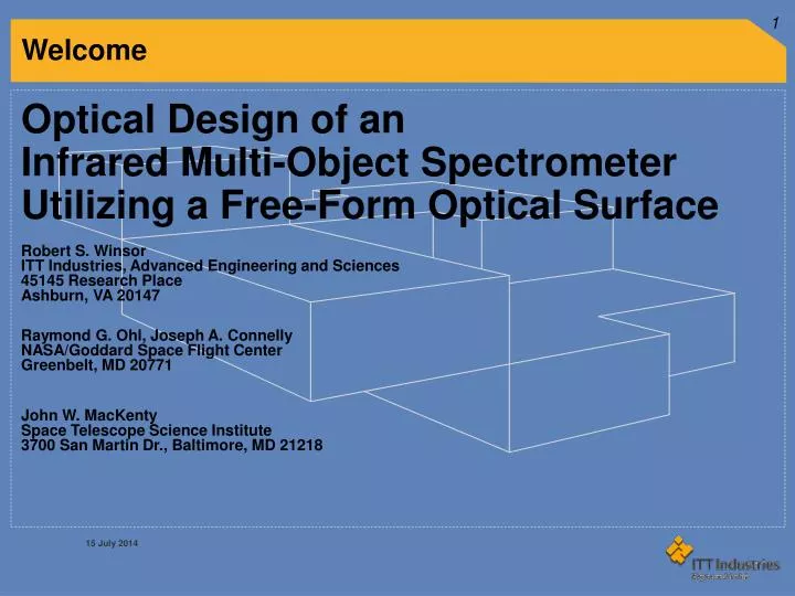
Optical Design of an Infrared Multi-Object Spectrometer Utilizing a Free-Form Optical Surface. Robert S. Winsor ITT Industries, Advanced Engineering and Sciences 45145 Research Place Ashburn, VA 20147 Raymond G. Ohl, Joseph A. Connelly NASA/Goddard Space Flight Center Greenbelt, MD 20771

E N D
Optical Design of an Infrared Multi-Object Spectrometer Utilizing a Free-Form Optical Surface Robert S. WinsorITT Industries, Advanced Engineering and Sciences45145 Research PlaceAshburn, VA 20147 Raymond G. Ohl, Joseph A. ConnellyNASA/Goddard Space Flight CenterGreenbelt, MD 20771 John W. MacKenty Space Telescope Science Institute 3700 San Martin Dr., Baltimore, MD 21218
Spetrometer • Schematic depiction of a Spectrometer
Multi-Object Spectrometers • Punch Plate • Take image • Make punch plate based on image • This is a sheet of opaque material with slit openings at the object locations • Install punch plate • Take observation data • Does not work well for spacecraft • Robotically positioned optical fibers • Integral field
Multi-Object Spectrometers • Punch Plate • Robotically positioned optical fibers • Mechanically complex and expensive • Limits ability to get spectra on neighboring objects simultaneously • Difficult to apply to an Infrared instrument • Cryogenic vacuum environment • Integral field
Multi-Object Spectrometers • Punch Plate • Robotically positioned optical fibers • Integral field • Small field of view • Maps fiber bundle to a vertical arrangement for imaging
MOS using a Micro-Mirror Array (MMA) • A programmable Slit MOS using a DMD • Using a Texas Instrument’s Digital Micromirror Device (DMD) for IRMOS • Mirrors are individually addressable into one of two tilt configurations (on or off) ±10º • A set of slits can be generated and implemented quickly • Flexibility in geometry of slit (good for galaxies) • 16mm square mirrors, 17mm mirror spacing • Allows for input focal ratios as fast as f/3.0 • 848 x 600 Mirror array
Micro-Mirror Array (MMA) Texas Instruments DMD GSFC MMAs
Micro-Mirror Array (MMA) • Design Challenges: • 10º Tilted Focal Plane • Clocked at 45 degrees • Discontinuous surface • Interference effects? • Wavefront error from spillover • Requires a User-Defined Surface for modeling in optical design software • These challenges are in addition to the typical challenges of a Multi-Object Spectrometer • Astigmatism is common in spectrometers of this type
Optical Design – Focal Reducer Front End • Designed for the Kitt Peak Mayall Telescope (3.8m) • Convert F/15 from telescope to f/4.6 • Plate scale = 0.2 arcsec/pixel • Seeing is typically 0.8”, and can be as good as 0.6” • Create tilted focal plane • Angle of incidence ~10 degrees at MMA • Spot sizes: FWHM better than 0.6” • Entirely Reflective
Optical Design - Spectrometer • Resolutions (Dl/ l) of 300, 1000, and 3000 in the J (1.1mm), H (1.6mm) and K (2.2mm) bands • Gratings have 50mm diameter active area • Spot sizes better than 0.6” FWHM • F/5.0 beam to detector • Rockwell HAWAII-I detector, 18.5mm pixels • Maintains 1:1 mapping from MMA to Detector • Compact size • Entirely Reflective
Correcting for Astigmatism • Traditionally, Toroidal surfaces are used. • Relatively easy to fabricate • Different radii of curvature (different power) in the “x” and “y” directions • Use conic values with toroidal shape to correct higher order wavefront error. • In “x” or “y” direction, but not both • Still straightforward to fabricate • Biconic • Different radii and conic values in both “x” and “y” directions
Biconic Mirror • Sagittal Depth given by the following:
IRMOS Front End Optics – Side View DMD M2 FoldMirror Telescope Focal Plane M1
IRMOS Front End Optics – Top View Dewar Window Cold StopPupil DMD
IRMOS Spectrometer Optics – Side View Biconic HAWAII-I Detector M3 Fold DiffractionGrating DMD
IRMOS Spectrometer Optics – Top View DiffractionGrating Filter M3 Biconic
IRMOS IRMOS Optics – Side View Biconic
IRMOS IRMOS Optics – Top View Biconic
IRMOS During I&T M3 Fold 1 M1 DiffractionGrating Wheel
Biconic Mirror (and Aspheric) Testing • Profilometry • Contact Method (discontinuous mapping) • Several hundred contact points • Relatively Low cost • Adequate accuracy? Perhaps. • Computer Generated Holograms (CGH) • Interferometric – continuous surface mapping • Relatively high cost compared with profilometry • Complex setup • How are the CGH’s tested? • More than adequate accuracy
IRMOS Fabrication Results • Biconic Fabrication Results White Light Interferometer110Ǻ RMS Micro-roughness UCMM Measurement:0.33 RMS ( = 632.8 nm) CGH Measurement:0.219 RMS ( = 632.8 nm)
IRMOS Fabrication Results • IRMOS has been assembled, and is in the cryostat • Spectra seen here in the Z-band (~800nm-1000nm) • Image is on a silicon mux, thus the fade in response • Width of spectra is ~7 pixels here. • This is an initial result. Further improvements are expected as additional tweaks are performed.
Conclusions • Using a free-form surface has made this instrument possible • The use of a free-form surface can be applied to a research-grade astronomical instrument • Trend in technology is making high-quality surfaces like these more accessible and affordable • Multiple metrology solutions are useful for determining surface errors to at least 60nm accuracy or better