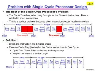
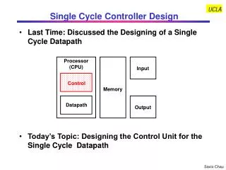
Download

1 / 10
100 likes | 337 Views
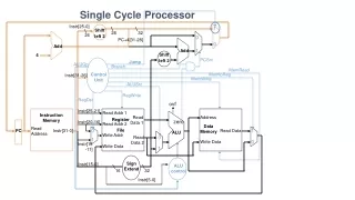
Single Cycle Processor Design using Verilog. module processor(Clock, Reset); input Clock, Reset; wire [31:0] PC_out, PC_In; //from pc wire [31:0] Instruction; //from instruction memory wire [31:0] IncPC; //from adder incrementing pc // from control unit

E N D
module processor(Clock, Reset); input Clock, Reset; wire [31:0] PC_out, PC_In; //from pc wire [31:0] Instruction; //from instruction memory wire [31:0] IncPC; //from adder incrementing pc // from control unit wire RegDst, RegWrite, ALUSrc, MemRead, MemWrite, MemToReg, Branch, Jump; wire [1:0] ALUOp; //from control wire [4:0] WriteAddr, JumpAddr; //from mux_reg wire [31:0] ReadData1, ReadData2; //from register wire [31:0] Out_signExtend; //from sign extension wire [31:0] In_B, In_shift, ShiftWire; //from alu muxs wire [3:0] In_Control; //from ALU control wire ShiftFunc, JR; wire [31:0] ALU_out; //from alu wire Zero, BranchType; //from alu wire [31:0] MemData; //from memory access wire [31:0] WriteData, JumpData; //from memory access mux wire [31:0] BranchAddress; //from branch adder wire [31:0] PC_Jump, JumpAddress, JumpAddress2; //from jump mux
PC PC_module(PC_out, PC_In, Clock, Reset); instructionMemory ins(Instruction, PC_out); adder_32bit increment_PC(IncPC, , , PC_out, 32'd4, 1'b0); controlUnit MainControl(ALUOp, RegDst, RegWrite, ALUSrc, MemRead, MemWrite, MemToReg, Branch, Jump, Instruction[31:26]); mux_2_1_5b mux_reg(JumpAddr, Instruction[20:16], Instruction[15:11], RegDst);
module PC(Out, In, Clock, Reset); output[31:0] Out; input [31:0] In; input Clock, Reset; reg [31:0] Out; initial begin Out = 32'd0; end always@(posedge Clock or posedge Reset) begin if(Reset == 1'b1) Out <= 32'd0; else Out <= In; end endmodule
module instructionMemory(ReadData, Address); output[31:0] ReadData; input [31:0] Address; reg [7:0] memory[512:0]; //512 locations of byte size memory reg [31:0] ReadData; //initialize memory (program in a sense) initial begin memory[0] <= 8'b00100100; //addiu $1, $0, 10 memory[1] <= 8'b00000001; memory[2] <= 8'b00000000; memory[3] <= 8'b00001010; memory[4] <= 8'b00100100; //addiu $1, $0, 15 memory[5] <= 8'b00000010; memory[6] <= 8'b00000000; memory[7] <= 8'b00001111; memory[8] <= 8'b00000000; //subu $3, $2, $1 memory[9] <= 8'b01000001; memory[10] <= 8'b00011000; memory[11] <= 8'b00100011;
.. …. .. . ……………// all instructions need to be examined memory[500] <= 8'b00000011; //jr $31 memory[501] <= 8'b11100000; memory[502] <= 8'b11111000; memory[503] <= 8'b00001000; ReadData <= {memory[0], memory[1], memory[2], memory[3]}; end //read and write memory always @ (Address) begin ReadData = {memory[Address], memory[Address+1], memory[Address+2], memory[Address+3]}; end endmodule
module adder_32bit (Sum, C_out, overflow, A, B, Mode); output [31:0] Sum; output C_out, overflow; input [31:0] A, B; input Mode; wire [31:0] Sum; wire C_out;
module controlUnit (ALUOp, RegDst, RegWrite, ALUSrc, MemRead, MemWrite, MemToReg, Branch, Jump, Instruction); input [5:0] Instruction; output [1:0] ALUOp; output RegDst, RegWrite, ALUSrc, MemRead, MemWrite, MemToReg, Branch, Jump; reg [1:0] ALUOp; reg RegDst, RegWrite, ALUSrc, MemRead, MemWrite, MemToReg, Branch, Jump; always@(Instruction) begin case(Instruction) 6'd0: begin //addu, subu, mult, div, and, or, xor, sll, sra, srl, slt, sltu, jr RegDst <= 1'b1; RegWrite <= 1'b1; ALUSrc <= 1'b0; MemRead <= 1'b0; MemWrite <= 1'b0; MemToReg <= 1'b0; Branch <= 1'b0; Jump <= 1'b0; ALUOp <= 2'b10; end
module mux_2_1_5b (Out, In0, In1, sel); output [4:0] Out; input [4:0] In0, In1; input sel; wire [4:0] Out; assign Out[0] = ~sel&In0[0] | sel&In1[0]; assign Out[1] = ~sel&In0[1] | sel&In1[1]; assign Out[2] = ~sel&In0[2] | sel&In1[2]; assign Out[3] = ~sel&In0[3] | sel&In1[3]; assign Out[4] = ~sel&In0[4] | sel&In1[4]; endmodule