Download
1 / 40
400 likes | 594 Views
Jump. R-Type. Load. Instr decode R read. Instr decode R read. ALU delay. Reg write. ALU delay. Mem read. Reg write. PC write. Instr Fetch. Instr Fetch. Instr Fetch. Instr Fetch. Instr Fetch. Instr Fetch. Instr decode. Time wasted. Time wasted. Time wasted. Clock. Clock.

E N D
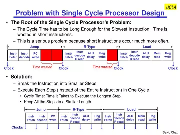
Jump R-Type Load Instr decode R read Instr decode R read ALU delay Reg write ALU delay Mem read Reg write PC write Instr Fetch Instr Fetch Instr Fetch Instr Fetch Instr Fetch Instr Fetch Instr decode Time wasted Time wasted Time wasted Clock Clock Clock Clock Jump R-Type Load Instr decode R read Instr decode R read ALU delay Reg write ALU delay Mem read Reg write PC write Instr decode Clocks Problem with Single Cycle Processor Design • The Root of the Single Cycle Processor’s Problem: • The Cycle Time has to be Long Enough for the Slowest Instruction. Time is wasted in short instructions. • This is a serious problem because short instructions occur much more often. • Solution: • Break the Instruction into Smaller Steps • Execute Each Step (Instead of the Entire Instruction) in One Cycle • Cycle Time: Time it Takes to Execute the Longest Step • Keep All the Steps to a Similar Length
Advantages and Complications of Multi Cycle Data Path • Advantages • Cycle time is much faster • Allows different instructions take different number of cycles to complete • Load takes five cycles • Jump only takes three cycles • Allows a functional unit to be used more than once per instruction • Complications • Need to add intermediate registers to hold data between steps • To Make Sure Intermediate Values Are Captured Before Next Clock • Need more complicate controller • Need to add more multiplexors for sharing function units
Clk Clk Purpose of Intermediate Registers Slow Clock R1 R2 0 1 X X 1 1 X . . . . . . . . . . . . 1 X 0 X 0 X 1 X 1 1 Fast Clock R1 R2 X X X X . . . . . . . . . . . . 1 X 0 X 0 X 1 X 1 1 R1 R2 Intermediate Register 1 0 1 X X 1 X . . . . . . . . . . . . 1 1 X 0 X 0 X 1 X 1 1 Clk
Instruction Fetch Decode/Operand Fetch Execute Possible places to put intermediate registers Access Memory Store Results Next Instruction But Where to Put the Intermediate Registers? • To Start With, Add the Intermediate Registers at the End of Each Step in the Instruction Execution Sequence Warning: Make Sure All Paths Between Intermediate Registers Have Similar Delays. Otherwise, the Overall Performance Can Be Worse Than Single Cycle Data Path!
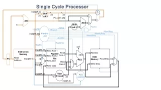
Control PC Basic Idea of Multi Cycle Data Path R-type 4 cycles Load 5 cycles Jump 3 cycles MemtoReg nPC_sel Op Code PC_Wr ALUctr ALUSrc IR_Wr MemWr RegDst RegWr ExtOp Store Result mux R A Exec Operand Fetch Instruction Fetch Next PC IR B M Memory Access
Additional logic Both Next address calculation Additional Logic Arithmetic Reuse of Function Units in Multi Cycle Data Path • Since intermediate results are stored in intermediate registers, function units can be doing different things at different time Examples: • Memory can be used to store both instructions and data • ALU can be used to do arithmetic and calculate branch address • Price to pay: extra registers (IR, ALUout) and multiplexors Instr Reg Load Instruction: PC Mem Data Reg Mem mux Instruction Fetch ALU Calculate Address mux Data address Read Memory Data PC Reg A PC PC mux 4 4 Reg A Reg file or mem Shift 2 ALUout Reg File Reg B Shift 2 bits for branch mux Reg B Instr IR Need to hold the output so ALU can be reused (15:0) Instruction (15:0) Single Cycle Data Path Multi Cycle Data Path
Dual- Port Ideal Memory • Dual Port Ideal Memory • Independent Read (RAdr, Dout) and Write (WAdr, Din) Ports • Read and Write (to Different Location) Can Occur at the Same Cycle • Read Port is a Combinational Path: • Read Address Valid • Memory Read Access Delay • Data Out Valid • Write Port is Falling Edge Triggered • MemWrite = 1 • Data In is Written Into Location[ WrAdr] at the Falling Clock Edge
General Steps to Design Multi Cycle Datapath Step 1: Start with a single cycle data path that is capable to perform all execution steps Step 2: Insert registers after each step in the instruction execution sequence. Make sure the delays in all steps are balanced. Step 3: Combine components if possible and add multiplexors Step 4: Work out clock by clock control signal sequence Note: Make sure IR is not changed before end of instruction See Example Questions 1 and 2
Critical Delay Path for add = 120 ns Critical Delay Path for lw = 170 ns Step 1: Start with a Single Cycle Data Path Example: A Single Cycle Data Path for add and lw PC+4 Next Address Logic PC 10 ns 20 ns Instruction Memory 20 ns R[rs] rs Rd add1 Data Memory rt Rd add2 Reg File ALU 0 mux Wr add R[rt] rd 1 mux imm16 0 Wr data 5 ns Read = 50 ns Write = 50 ns Read = 30 ns Write = 30 ns 1 50 ns 5 ns ext 0 20 ns mux 1 5 ns Assume all control signals arrive before data: Delay for add: 10 + 50 + 30 + 5 + 20 + 5 = 120 ns Delay for lw: 10 + 50 + 30 + 5 + 20 + 50 + 5 = 170 ns Clock Cycle of Data Path = 170 ns Execution Time for add = 1 clock 170 ns/clock = 170 ns Execution Time for lw = 1 clock 170 ns/clock = 170 ns
Step 2: Insert Intermediate RegistersExample:Insert Registers Without Considering Delays PC+4 Next Address Logic PC 10 ns 20 ns Instruction Memory 20 ns R[rs] rs A Rd add1 Data Memory rt Rd add2 ALU Out Reg Mem Data Reg Reg File 10 ns ALU 0 Instr Reg mux Wr add R[rt] rd B 1 mux imm16 0 Wr data 5 ns Read = 50 ns Write = 50 ns 10 ns 10 ns 10 ns Read = 30 ns Write = 30 ns 1 50 ns 10 ns 5 ns ext 0 20 ns mux 1 5 ns For add: PC Instr Mem out = 10 + 50 = 60 ns Instr Reg B reg = 10 + 30 = 40 ns (mux not in critical path since not writing yet) B reg ALU output = 10 + 5 + 20 = 35 ns ALUOut Reg Reg File Written = 10 + 5 + 30 = 45 ns (IR can’t be updated till Reg File is written) For lw: PC Instr Mem out = 10 + 50 = 60 ns Instr Reg B reg = 10 + 5 + 30 = 45 ns B Reg ALU output = 10 + 5 + 20 = 35 ns ALU Out Reg Memory output = 10 + 50 = 60 ns Mem Data Reg Reg File Written = 10 + 5 + 30 = 45 ns (IR can’t be updated till Reg File is written) Clock cycle = longest stage = 60 ns Execution time for add = 4 clocks x 60 ns/clock = 240 ns PC updated during last instruct execution Execution time for lw = 5 clocks x 60 ns/clock = 300 ns PC updated during last instruct execution
Step 2: Insert Intermediate RegistersA More Balanced Multi-Cycle Data Path PC+4 Next Address Logic PC 10 ns 20 ns Instruction Memory 20 ns R[rs] rs Rd add1 Data Memory rt Rd add2 ALU Out Reg Mem Data Reg Reg File ALU 0 Instr Reg mux Wr add R[rt] rd 1 mux imm16 0 Wr data 5 ns Read = 50 ns Write = 50 ns 10 ns 10 ns Read = 30 ns Write = 30 ns 1 50 ns 10 ns 5 ns ext 0 20 ns mux 1 5 ns For add: PC Instr Mem out = 10 + 50 = 60 ns Instr Reg ALU output = 10 + 30 + 5 + 20 = 65 ns ALUOut Reg Reg File Written = 10 + 5 + 30 = 45 ns (IR can’t be updated till Reg File is written) For lw: PC Instr Mem out = 10 + 50 = 60 ns Instr Reg ALU output = 10 + 30 + 5 + 20 = 45 ns ALU Out Reg Memory output = 10 + 50 = 60 ns Mem Data Reg Reg File Written = 10 + 5 + 30 = 45 ns (IR can’t be updated till Reg File is written) Clock cycle = longest stage = 65 ns Execution time for add = 3 clocks x 65 ns/clock = 195 ns PC updated during last instruct execution Execution time for lw = 4 clocks x 65 ns/clock = 260 ns PC updated during last instruct execution Note: The add instruction is faster than the single cycle data path but lw is slower
Step 2: Insert Intermediate RegistersEffect of Register Locations PC+4 Next Address Logic PC 10 ns 20 ns Instruction Memory 20 ns R[rs] rs Rd add1 Data Memory rt Rd add2 ALU Out Reg Mem Data Reg Reg File ALU 0 Instr Reg mux Wr add R[rt] rd 1 mux imm16 0 Wr data 5 ns Read = 50 ns Write = 50 ns 10 ns 10 ns Read = 30 ns Write = 30 ns 1 50 ns 10 ns 5 ns ext 0 20 ns mux 1 5 ns For add: PC Instr Mem out = 10 + 50 = 60 ns Instr Reg Reg File Written = 10 + 30 + 5 + 20 + 5 + 30 = 100 ns For lw: PC Instr Mem out = 10 + 50 = 60 ns Instr Reg ALU output = 10 + 30 + 5 + 20 = 45 ns ALU Out Reg Memory output = 10 + 50 = 60 ns Mem Data Reg Reg File Written = 10 + 5 + 30 = 45 ns Clock cycle = longest stage = 100 ns Execution time for add = 2 clocks x 100 ns/clock = 200 ns PC updated during last instruct execution Execution time for lw = 4 clocks x 100 ns/clock = 400 ns PC updated during last instruct execution Note: The add instruction is faster than last design but lw is much slower
Observation • For single cycle data path Execution Time for add = 1 clock 170 ns/clock = 170 ns Execution Time for lw = 1 clock 170 ns/clock = 170 ns • For multi-cycle data path Case 1: 4 levels of intermediate registers Execution time for add = 4 clocks x 60 ns/clock = 240 ns Execution time for lw = 5 clocks x 60 ns/clock = 300 ns Case 2: 3 levels of intermediate registers Execution time for add = 3 clocks x 65 ns/clock = 195 ns Execution time for lw = 4 clocks x 65 ns/clock = 260 ns Case 3: 3 levels of intermediate registers, new location for ALUout Reg Execution time for add = 2 clocks x 100 ns/clock = 200 ns Execution time for lw = 4 clocks x 100 ns/clock = 400 ns • Observations: • 1. All multi-cycle data paths are slower than the single cycle data path! • Reason: The lw path length is not much longer than the path length for add. In order for a multi-cycle data to have significant performance over single cycle data path, the path length of long instructions has to be much longer than short instructions. (In fact, if all instructions have the same path length, the multi-cycle data path is always worse than a single cycle data path.) • Case 2 has the best performance among the multi-cycle data path. • Reason: it has the most balanced data path among the multi-cycle data path.
Data Memory Mem Data Reg Step 3: Combining Components PC+4 Next Address Logic PC Instruction Memory R[rs] rs A Rd add1 rt Rd add2 ALU Out Reg Reg File ALU 0 Instr Reg mux Wr add R[rt] rd B 1 mux imm16 0 Wr data 1 ext 0 mux 1
mux Step 3: Combining Components PC+4 Next Address Logic PC Instruction Memory R[rs] rs A Instruction and data Memory Rd add1 rt Rd add2 ALU Out Reg Reg File ALU 0 Instr Reg mux Wr add R[rt] rd B 1 mux imm16 0 Wr data 1 ext 0 mux 1 Mem Data Reg
Describing Multi-Cycel Data Path with Multi Cycle RTL • Group all RTL statements by clock • All register transfers in the same clock occur simultaneously Example: Multi Cycle RTL for the add Instruction Execution SequenceClockRTL Instruction Fetch: 1 IRMem[PC] PC PC + 4 Operand Fetch: 2 rs IR<25:21> rt IR<20:16> rd IR<15:11> RA R[rs] RBR[rt] Execute: 3 ALUOUT RA + RB Store Result: 4 R[rd] ALUOUT Compare to Single Cycle RTL for the add Instruction instr mem[PC] rs instr<25:21> rt instr<20:16> rd instr<15:11> R[rd] R[rs] + R[rt] PC PC + 4
Operation Details of Multi Cycle Data Path Will Look at the Details of Each Step in the Instruction Execution Sequence: • Step 1: Instruction Fetch • Step 2: Instruction Decode and Register Fetch • Step 3: Execution, Memory Address Computation, or Branch Completion • Step 4: R-Type Completion or Memory Access for Load/Store Instructions • Step 5: Memory Read and Load Completion
Cycle Ends AT the Next Clock Tick • IRmem[PC]; PC<31: 0> PC<31: 0> + 4 • Cycle Begins Right AFTER the Clock Tick • Instr Reg mem[PC]; PC<31: 0> + 4 PC+12 PC+8 PC+8 PC+4 Instruction Fetch Step One Clock Cycle ALUOp= Add, ALUSrcB= 01 x: PCWrCond, RegDst, MemtoReg, ExtOp 1: PCWr, IRWr; Others: 0 PC+4
Idle Minimal Functionality Required forInstruction Decode and Register Fetch Step
Use the idle components to do something useful: branch address calculation Decoding of Branch-if-Equal (beq) Instruction:Simultaneously Preparing for Branch Address ALUOp= Add, ALUSrcB= 11 1: ExtOp x: RegDst, PCSrc, IorD, MemtoReg Others: 0 Motivation: To take advantage of the idle components while decoding instruction to save one more cycle if the instruction happens to be a branch
If Branch Actually Occurs in Execution Step Registers holding operand when execution step begins Holding branch address computed during instruction decode
R-Type Instruction Decode Step Branch address preparation as discussed before (result may not be used but it is harmless if ALUout is not written to other state elements)
instruction is not a branch, pre-calculated branch address is overwritten by the add instruction R- Type Completion Step
Store Instruction Execution Step (Memory Address Calculation)
Load Instruction Execution Step (Memory Address Calculation)
Jump Instruction Decode and Complete Steps • • PC_ incr PC + 4 • PC<31: 2> PC_ incr<31: 28> concat target<25: 0> JComplete 1: PCWrite PCsrc = 10 x: others PCwr = 1 PCWr=1 PCsrc=2 PCsrc = 2 2 1 0 J Instr<25:0> PC<31:28> 4 26
Putting it all Together: Multiple Cycle Datapath PCsrc 2 1 0 MUX
Reg File RegWr Ra 5 busA Ra 32 5 Rw 5 busB busW 32 32 Memory WrEn Adr 32 Din Dout 32 32 Race Condition Between Address and Write Enable • This “Real” (no clock input) Register File may not Work Reliably in our Design Because: • We cannot Guarantee Rw will be Stable one “Set- up” Time BEFORE RegWr= 1 • There is a “race” between Rw (address) and RegWr (write enable) • The “Real” (no clock input) Memory may not Work Reliably in our Design Because: • We cannot Guarantee Address will be Stable one “Set- up” Time BEFORE WrEn = 1 • There is a race between Addr and WrEn
Delay WrEn Memory WrEn Addr reg Adr 32 Clock Data reg Din Dout 32 32 How to Avoid this Race Condition? • A Possible Solution: • Have A Register Attached Directly to the Address and Data Inputs • Store Address and Data info at the End of Cycle N • Assert Write Enable Signal with Combinational Logic Delay into Cycle (N+ 1) where: Delay into Cycle N+1 clock- to- Q + setup • Disadvantage: • Extra Register Delay • Extra Logic Circuit