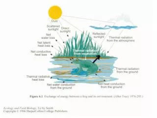
Download
1 / 3
30 likes | 188 Views
Electrons on the brink: Fractal patterns may be key to semiconductor magnetism Ali Yazdani, Princeton University, DMR 0704314.

E N D
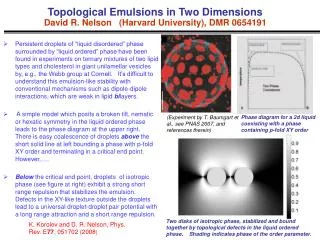
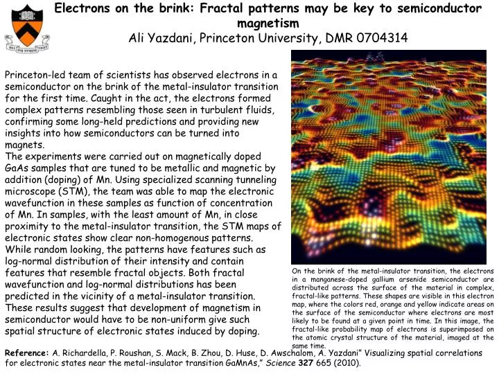
Electrons on the brink: Fractal patterns may be key to semiconductor magnetismAli Yazdani, Princeton University, DMR 0704314 Princeton-led team of scientists has observed electrons in a semiconductor on the brink of the metal-insulator transition for the first time. Caught in the act, the electrons formed complex patterns resembling those seen in turbulent fluids, confirming some long-held predictions and providing new insights into how semiconductors can be turned into magnets. The experiments were carried out on magnetically doped GaAs samples that are tuned to be metallic and magnetic by addition (doping) of Mn. Using specialized scanning tunneling microscope (STM), the team was able to map the electronic wavefunction in these samples as function of concentration of Mn. In samples, with the least amount of Mn, in close proximity to the metal-insulator transition, the STM maps of electronic states show clear non-homogenous patterns. While random looking, the patterns have features such as log-normal distribution of their intensity and contain features that resemble fractal objects. Both fractal wavefunction and log-normal distributions has been predicted in the vicinity of a metal-insulator transition. These results suggest that development of magnetism in semiconductor would have to be non-uniform give such spatial structure of electronic states induced by doping. On the brink of the metal-insulator transition, the electrons in a manganese-doped gallium arsenide semiconductor are distributed across the surface of the material in complex, fractal-like patterns. These shapes are visible in this electron map, where the colors red, orange and yellow indicate areas on the surface of the semiconductor where electrons are most likely to be found at a given point in time. In this image, the fractal-like probability map of electrons is superimposed on the atomic crystal structure of the material, imaged at the same time. Reference:A. Richardella, P. Roushan, S. Mack, B. Zhou, D. Huse, D. Awschalom, A. Yazdani” Visualizing spatial correlations for electronic states near the metal-insulator transition GaMnAs,” Science327 665 (2010).
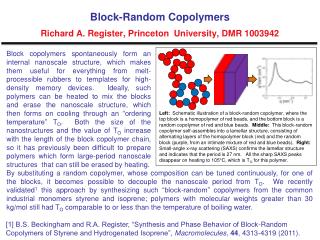
Topological Protection Against BackscatteringAli Yazdani, Princeton University, DMR 0704314 Topological insulators are a new class of insulators in which a bulk gap for electronic excitations is generated by strong spin-orbit coupling. These novel materials are distinguished from ordinary insulators by the presence of gapless metallic boundary states, akin to the chiral edge modes in quantum Hall systems, but with unconventional spin textures. A key characteristic of these spin-textured boundary states is their insensitivity to spin-independent scattering, which protects them from backscattering and localization. We use a scanning tunneling microscope (STM) to visualize the gapless surface states of the three-dimensional topological insulator Bi1-xSbx and to examine their scattering behavior from disorder caused by random alloying in this compound. Combining STM and angle-resolved photoemission spectroscopy, we show that despite strong atomic scale disorder backscattering between states of opposite momentum and opposite spin is absent. Our observation of spin-selective scattering demonstrates that the chiral nature of these states protects the spin of the carriers; they therefore have the potential to be used for coherent spin transport in spintronic devices. Electrons in topological insulator BiSb scatter from alloying defects leaving distinct signatures in the Fourier transform of the STM measured LDOS. These FFT maps show a absence of waavevector connecting k to –k for surface wave scattering hence proving absence of backscattering Reference: P. Roushan, J. Seo, C. V. Parker, Y.-S. Hor, D. Hsieh, D Qian, A. Richardella, M. Z. Hasan, R. J. Cava and A. Yazdani “Topological Surface States Protected From Backscattering by Chiral Spin Texture,” Nature 460 1106 (2009).
Topological Surface States Penetrate Through Surface Barriers Ali Yazdani, Princeton University, DMR 0704314 high low Topological surface states are a new class of novel electronic states that are potentially useful for quantum computing or spintronic applications. Unlike conventional two-dimensional electron states, these surface states are expected to be immune to localization and to overcome barriers caused by material imperfection. Previous experiments have demonstrated that topological surface states do not backscatter between equal and opposite momentum states, due to their chiral spin texture. However, to date there is no evidence as to whether these states in fact transmit through natural occurring surface defects and consequently are connected on the exterior of a bulk sample regardless of its shape. We used a scanning tunneling microscope to measure transmission and reflection probability of Sb’s topological surface states through naturally occurring crystalline steps separating atomic terraces. In contrast to non-topological surface states of common metals (Cu, Ag, Au), which are either reflected or absorbed by atomic steps, we show topological surface states of Sb to penetrate through such barriers with high probability. This demonstration of the extended nature of Sb’s topological surface states suggests that such states may be useful for high current transmission even in the presence of atomic scale irregularities—an electronic feature sought to efficiently interconnect nanoscale devices. STM Topograph Spectroscopic Map 0 110 Energy (meV) Building a Fabry-Perot Interferometer for topological surface states. Evidence for transmission of the surface state can be seen in flat terrace at specific energies (arrows). Similar barriers fully reflect conventional surface state (Cu, Ag, Au). Experiments such as this demonstrate that in Sb the probability for transmission and reflection are about equal at 40%. In Sb the presence of a hole pocket makes it possible that there is a reflection, which is advantages as it allows both transmission & reflection to be measured using the STM. Distance (Å) Reference: J. Seo, P. Roushan, . Beidenkopf,, R. J. Cava and A. Yazdani “Transmission of Topological Surface States Through Surface Barriers” Nature 466 434 (2010).