Download
1 / 33
330 likes | 514 Views
Digital Camera Trigger Status. December 2013 K.-H. Sulanke DESY. Introduction. Design for MST (Medium Size Telescopes) and possibly also for LST (Large Size Telescopes) Because of the NSB (Night Sky Background), the trigger design is quite challenging

E N D
Digital Camera TriggerStatus December 2013 K.-H. Sulanke DESY K.-H. Sulanke, DESY
Introduction Design for MST (Medium Size Telescopes) and possibly also for LST (Large Size Telescopes) Because of the NSB (Night Sky Background), the trigger design is quite challenging Single pixel rate can be greater than 100 Mhz Basic requirements are Sensitive for weak PMT signals Fast Low latency Low power Cheap Alternative to the „Analog Trigger“ designed by Spanish colleagues Based on analog sums of up to 21 pixel Theoretically better for weak and noisy signals (LST) 9/19/2014 K.-H. Sulanke, DESY 2
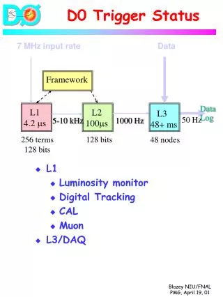
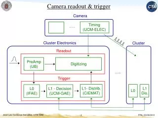
Principle Three stage trigger L0 is a high speed PMT-pulse discriminator L1 trigger is based on a single, low cost FPGA, processing 37 pixel areas L2 is seperate crate, generating the camera trigger 9/19/2014 K.-H. Sulanke, DESY 3
37 Pixel Trigger Regions 7 cluster trigger region • clusters of a MST shown • Each heagon represents 7 pixel • the trigger region overlaps by four pixels always 9/19/2014 K.-H. Sulanke, DESY 4
37 Pixel Trigger Region 15 f 10 62 a c 12 14 60 c e a 25 13 63 65 f d d f 76 64 24 g e e 20 71 52 75 a b c f 23 70 53 d a d 22 72 74 50 c c e a 34 73 54 e d e 35 55 33 43 f f d d 30 44 42 a e c 32 40 c a 45 f 9/19/2014 K.-H. Sulanke, DESY 5
The Trigger Schema L2 DTB 24V (optional) L0_neighbor CSB L1 L2CB FEB 7 7 #01 L0 GPS_clock Sector_trig PMT #01 ethernet FPGA … L0_neighbor … L1 FPGA FEB FPGA #18 7 #16 7 L0 Camera_trig PMT FPGA PMT = Photomultiplier Tube FEB = Frontend Board DTB = Digital Trigger Backplane CSB = Cluster Service Board L2CB = L2 Controller Board 9/19/2014 K.-H. Sulanke, DESY 6
Digital Trigger L0 Mezzanine Board Schematic simulated LMH6629, very low noise, low offset preamplifier Analog input signal range down to 1mV Digital L0 Mezzanine Comp Opamp LVDS DAC Diff. Analog in LVDS out Preamp LVDS Comparator Trigger threshold 9/19/2014 K.-H. Sulanke, DESY 7
Digital Trigger L0 Mezzanine Board 6 layer PCB with length-tuned signal lines Preamplifier Comparator Trigger- Treshold-DAC 9/19/2014 K.-H. Sulanke, DESY 8
L0, minimum analog input Level Diff. Analog in Discr., LVDS out 9/19/2014 K.-H. Sulanke, DESY 9
L1, Digital Trigger Backplane Rev. 2 RJ-45 ethernet Frontend board connector ethernet power CLK PPS L0_trigger trigger IP_addr HV_ena SPI / JTAG calib_cyc reserved 24V power vreg clock (opt.+power) PPS L1_trigger_out L2_trigger_in flash osc RJ-45 Xilinx FPGA flash L0 in /out and ... connectors to neighbor clusters 9/19/2014 K.-H. Sulanke, DESY 10
The L1-FPGA‘s Functionality delay delay delay delay delay delay delay FPGA FPGA FPGA FPGA FPGA FPGA FPGA Xilinx Spartan 6 FPGA fanout to surrounding clusters from center cluster pix_[0][6..0] pix*_[0][4..0] calibrate STM progr. delays from surrounding clusters 37 pixel trigger fabric to L2_trigger board pix_[1][4..0] trigger pix_[6][4..0] clock PLL 9/19/2014 DESY 11
Digital Trigger Backplane, 8 Layer PCB PCB design by Carola Rueger DESY 9/19/2014 K.-H. Sulanke, DESY 12
Digital Trigger Backplane, cont. Test Port Xilinx JTAG port Cluster-Position- ID switches FE-board Gigabit port Xilinx Spartan-6 FPGA Power_in Clock_in PPS_in L1_out L2_in 64 bit ID ROM Local Oscillator Alternative power connector Temp. sensor FE-board 24V-fuse Atmel PROM (Xilinx config.) neighbor cluster connections FE-Board connector Local synchronous DC-DC power supply 9/19/2014 K.-H. Sulanke, DESY 13
L1, Connecting the Trigger Backplanes PCB design by Carola Rueger DESY 9/19/2014 K.-H. Sulanke, DESY 14
Combined Power and Clock Input 24V, clock, and PPS over a single wire pair requires a single cat5e cable per cluster only (+ gigabit ethernet cable) Current spikes of 0.8 A did not influence the (recovered) clock quality Ext_Clock_PPS Clock_recovered PPS_recovered 24V Alternative Power conn. Clock+pps Combined Power and Clock input FE-board Gigabit port 9/19/2014 K.-H. Sulanke, DESY 15
Digital Trigger Backplane, Status 7 boards assembled by the DESY workshop Tests : Power supply √ Xilinx configuration via JTAG or PROM √ Local and external clock √ LVDS Interface (signal integrity) to neighbor clusters √ Inverse mode (for testing), used as a 37 bit pattern generator √ Minimum (clean) signal width is 1.25 ns Combined power / clock / pps / L1_out / L2_in RJ45-connection √ Saves cabling Various trigger alghorithms (firmware), 3NN done Temperature sensor, - Serial backplane 64bit address PROM (FEB ethernet MAC), - FE-board interface , √ 9/19/2014 K.-H. Sulanke, DESY 16
Digital Trigger Test Board Testing the L0 boards AND the FE-board interface of the Dig. Trigger Backplane Xilinx with RS232 / RS485 interface, to set the discriminator thresholds etc. Dig.Trigger-Bpl. 6x5 L0 by surr. clusters L0-Testboard Single ended to diff. Digital L0 Mezzanine FPGA PMT or Pulse-Gen. Comp 7 L0 Opamp Opamp LVDS FPGA DAC RS 232 RS 485 FE-board interface 9/19/2014 K.-H. Sulanke, DESY 17
Digital Trigger Test Setup 120 mm x 260 mm, 6 Layer PCB, various analog and digital test points L1 Trigger Backplane L0 Testboard RS232 / 485 interface L0-Mezzanine Xilinx Analog Inputs 9/19/2014 K.-H. Sulanke, DESY 18
3NN Trigger Test Setup pulse generator (..4 delayed outputs) USB to RS485 Terminal to set L0 thresholds L1, backplanes, center cluster RS485 port 40 dB attenuators to get 5mV Testboards with L0 mezzanines JTAG-chain Testboard + L1 backplane Axels Clock fanout Trigger signal K.-H. Sulanke, DESY
3NN Trigger Test Results 100% trigger and 0% trigger situation 5mV pk 2.5 ns FWHM 3ns shift trigger No trigger • Analog input signals, zoomed time scale 9/19/2014 K.-H. Sulanke, DESY 20
First 3NN Trigger Firmware Revision 3NN of 37 pixel Firmware automatically detects missing neighbors Fully synchronous design „plug and play“ version runs from local oscillator (25 Mhz) Sampling rate 750 Mhz Based on pulse shaped L0 signals of 2.6 ns lengths Trigger latency 120 ns Trigger time resolution 1.3 ns Trigger jitter +/- 1.3 ns Test setup with 3 connected clusters all 3NN combinations checked using PMT like signals (5mV pk) also 100 Mhz global clock tested 9/19/2014 K.-H. Sulanke, DESY 21
L2 L2 still in the design phase based on Xilinx-Spartan 6 FPGAs will be a crate, ~ 50 x 20 x 20 cm, ~ 11 kg 18 x CSB (Cluster Service Board) 1 x L2CB (L2 Controller Board) Ethernet interface Optical / electrical camera trigger output L2 DTB 24V (optional) L0_neighbor CSB L1 L2CB FEB 7 7 #01 L0 GPS_clock Sector_trig PMT #01 ethernet FPGA … L0_neighbor … L1 FPGA FEB FPGA #18 7 #16 7 L0 Camera_trig PMT FPGA PMT = Photomultiplier Tube FEB = Frontend Board DTB = Digital Trigger Backplane CSB = Cluster Service Board L2CB = L2 Controller Board 9/19/2014 K.-H. Sulanke, DESY 22
L2, Cluster Service Board (CSB) vreg flash 16 x Cat5e cables RJ45 RJ45 RJ45 RJ45 RJ45 RJ45 RJ45 RJ45 RJ45 RJ45 RJ45 RJ45 RJ45 RJ45 RJ45 RJ45 Cur_mon 16 x switch Clock PPS L1_trigger L3_trigger Xilinx FPGA Or optional, including 24V 24V CLK PPS L2 L3 sdat JTAG Clock_PPS_24V GND L1_trigger L3_trigger Backplane connector 9/19/2014 K.-H. Sulanke, DESY 23
L2 Trigger Sectors, MST, Example 271 cluster shown (1897 pixel) Each sector comprises 14..16 clusters and is connected to a certain L2 board („CSB“) 9/19/2014 K.-H. Sulanke, DESY 24
Summary Main advantage of the digital trigger is its flexibility concerning the trigger algorithm and the simplicity of the overall scheme The first two stages of the digital trigger have been designed and tested The L0 stage performs very good (signals of 1mV are still detectable) First results with the L1 stage, e.g. the 3NN trigger, are encouraging More sophisticated alghorithms will follow E.g. a time gradient trigger The L2 stage will be designed and tested in 2014 Intermediate solution (by Axel Kretzschmann) do exist First camera integration tests in 2014 Not yet clear who makes it finally, the analog or the digital trigger ? 9/19/2014 K.-H. Sulanke, DESY 25
Outlook 19 cluster „Demonstrator“ test planned in Q4 2014 with DragonCam (LST, Japan) DRS4 based (Domino Ring Sampler Rev4, analog pipeline chip) and NectarCam (MST, France) Nectar chip based (analog pipeline chip) 9/19/2014 K.-H. Sulanke, DESY 26
Back Up Slides 9/19/2014 K.-H. Sulanke, DESY 27
Test Setup w. Pattern Generator expected and real trigger trigger board pattern generator board 9/19/2014 K.-H. Sulanke, DESY 28
Digital Trigger Backplane, List of Key Hardware Features • Nominal power consumption: 1.5 W • Weight : 95 g + 10 g cabling to neighbor clusters -> 28 kg for LST • Automatic neighbor cluster recognition (border zone) • Synchronous DC-DC converter (24 V to 3.0 V …) • Local clock and external clock input (any diff. > 0.1V pk-pk) • FPGA load by JTAG cable or PROM or remote (by FE board) • 6 x bidirectional L0 signal connection with neighbor cluster • Temperature sensor (allows automatic delay correction, if needed) • adjustable 8 bit cluster position ID (for unique, position-independant, firmware) • Gigabit ethernet pass through connection to FE-board • RJ 45 connector as combined power and clock input (single cat5e cable) K.-H. Sulanke, DESY
M12 Cat6 , Combined Power / Clock Input • Instead of RJ45, more robust • by Harting, Molex, ... To be replaced by M12 9/19/2014 K.-H. Sulanke, DESY 30
7-PMT-Cluster “DragonCam” K.-H. Sulanke, DESY
The MST Camera • PMT based • Pixel-d : 38 mm (1.5 Zoll, z.B. Hamamatsu PMT R11920-100) • Pixel-grid : 50 mm • 1771 Pixel, ~253 Cluster a´ 7 Pixel • Size of the pixel-array : ~ 2 qm • Weight : .. 2000 kg • Extrem fast and extrem light sensitive • „shutter“ time in the ns region K.-H. Sulanke, DESY
Analog Pipeline Chip • 500 MHz ... 5 GHz sampling rate K.-H. Sulanke, DESY