Download
1 / 15
150 likes | 153 Views
This summary provides an update on the status of DØ Alpha hardware, including difficulties with MBus PIO, arbitration problems, and the development of a firmware patch. It also introduces the concept of Beta hardware as an Alpha replacement and outlines the timeline for the project.

E N D
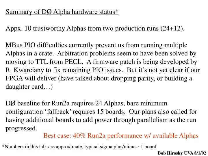
Summary of DØ Alpha hardware status* Appx. 10 trustworthy Alphas from two production runs (24+12). MBus PIO difficulties currently prevent us from running multiple Alphas in a crate. Arbitration problems seem to have been solved by moving to TTL from PECL. A firmware patch is being developed by R. Kwarciany to fix remaining PIO issues. But it’s not yet clear if our FPGA will deliver (have talked about dropping parity, or building a daughter card…) DØ baseline for Run2a requires 24 Alphas, bare minimum configuration ‘fallback’ requires 15 boards. Our plans also called for having additional boards to add power through parallelism as the run progressed. Best case: 40% Run2a performance w/ available Alphas *Numbers in this talk are approximate, typical sigma plus/minus ~1 board Bob Hirosky UVA 8/1/02
Enter the betas: Alpha replacement Originally proposed at end of 2000 to cover DØ in case of major shortfall in Alpha production + provide clear upgrade path & reduce dependence on component lifetimes (rapid obsolescence). • Beta designed w/ several goals in mind: • Turn around time (~ 18mo from settling design to full production) • Low Risk • Plug-in hardware compatibility w/ Alphas • Minimal impact on software infrastructure • Minimal drain on Run2a commissioning efforts • Easy upgrades Bob Hirosky UVA 8/1/02
Timescale for Project: • May 2001 - finalize design, start schematics • Feb 2002 - first prototype • Jun 2002 - order pre-production samples • Now - pre-production board checks • Sep/Oct 2002 - Start production • Dec/Jan - Install in trigger • Firmware effort started ~Dec01 expected to finish ~Oct/Nov02 • part time efforts of ~1.5 Engineers (est. 30% on project) Web link for details on L2beta (TDR, etc): http://galileo.phys.virginia.edu/~rjh2j/l2beta/ Bob Hirosky UVA 8/1/02
‘L2ßeta’ CPU Same Basic Concept as L2Alpha, but with simplified implementation Keep UII Modern FPGA/ PCI interface replaces: DMA PIO TSI device Just add drivers… Keep ECL drivers Buy this and get a warranty! Bob Hirosky UVA 8/1/02
Basic Idea • PIII Compact PCI card • 9U card with “custom” devices (3 BGA’s) • Universe Chip VME interface • commercial 64-bit PCI interface chip • MBus and other logic in FPGA 9U board 64 bit J5 6U board <2MHz VME Compact PCI Drivers J4 UII J3 32 bits J2 66 MHz (max) 64 bits Local bus PLX 33 MHz 9656 PCI J1 Clk (s)/ FPGA Drivers roms ECL Drivers 128 bits ~20 MHz MBus Bob Hirosky UVA 8/1/02
What is the PLX and we did we use it? The PLX is a hardware PCI interface that provides a simplified local bus data protocol. Supports 64/66MHz on PCI, 32/66MHz on LBus. Local and PCI buses are asynchronous. Simplified DMA model. Setup the PLX w/ source & target addresses, it masters both buses and controls the transaction. No need to deal w/ PCI core implementation, reduce firmware risk. Bob Hirosky UVA 8/1/02
Feb ‘02 Level 2 beta: 1st assembled prototype Bob Hirosky UVA 8/1/02
New/Improved features: • 3x CPU performance + • >2x on chip cache Cheap upgrade = add 2nd CPU* *but SW not trivial Bob Hirosky UVA 8/1/02
Estimated DMA rates adding 3 PCI + 3 Local clocks for arbitration, Numbers in () do include the Local clocks • Further speedup options: • Place UII behind a bridge allowing 66MHz bus on 9U card • Replace PLX w/ PCI core Bob Hirosky UVA 8/1/02
FPGA: Xilinx XCV405E (Virtex extended memory) FPGA resources used (approximate): I/O pins 359/404 Block Ram 69K/70K Other resources <25% Most functions implemented, still need DMA engine and some mapper code. Bob Hirosky UVA 8/1/02
DØ compatibility: HW: plug-in Alpha replacement . SW: rewrite device level code, high level framework/algorithms essentially unaffected by the switch over, just recompile on PIII hardware.* System: Linux 2.4.x kernel add Ext3 file system add memory management module will test ‘real time’ scheduler patch, improved profiling, etc available for PIII *Software compatibility is a huge benefit of going with betas for DØ. This project would not have been feasible on the Run2a timescale if software impacts we large. Bob Hirosky UVA 8/1/02
Issues for CDF Adaptation • Hardware: • We have moved to a full TTL MBUS (removed 4 PECL drivers) • A smaller subset of J2 user I/O pins connected ~ 24 CDF specific signals unconnected on Beta. 1-2(?) signals may have reversed direction… • Front panel output is ECL, not LVDS (it’s output only, but I/O can be set for each pin in firmware • Layout design on Cadence (LAL Group in Orsay) • Software: • ??? (As far as a DØ character can guess!) Bob Hirosky UVA 8/1/02
Issues for CDF Adaptation (continued) • Firmware: • MBUS PIO should be equivalent, TSI functions are essentially the same save the unconnected pins (CDF specific regs, not implemented) • All FW written in Verilog - no PCI code & 1 design tool! • DMA/Broadcast Firmware is quite different. Data FIFO same, but: • 9 bits of DMA address supported (vs 10 on Alpha) • Address FIFO replaced by addr. change and counter fifos • (assumes >= 4MB words/per each MB broadcast • DMA engine waits for a source to complete and tells the • PLX to initiate a burst of a known size. • Fifo input rate – fast enough? (Dstrobe + ~30ns now, shooting for 25…) • (Alpha FIFO scheme could be implemented in our FPGA if broadcast addresses limited to 8 bits, else $500 more buys a bigger chip w/ same footprint. Higher speed grades also available.) Bob Hirosky UVA 8/1/02
Cost Estimate: 1Q02 In-kind contribution from LAL for Engineeering Assembled by Thales in France -Mech. design -PCB test -Jtag test SBCs have been coming down in price, but price range is large… we expect to shave $1K+ off SBC+disk combo…Just over $5K/board – production price Bob Hirosky UVA 8/1/02
21st Century approach… What if we were starting from a completely clean slate? Might consider Vertex Pro series – CPU + FPGA on chip No need to mess / PCI, communicate w/ CPU through shared memory Very simple board design Bob Hirosky UVA 8/1/02