Download
1 / 34
350 likes | 482 Views
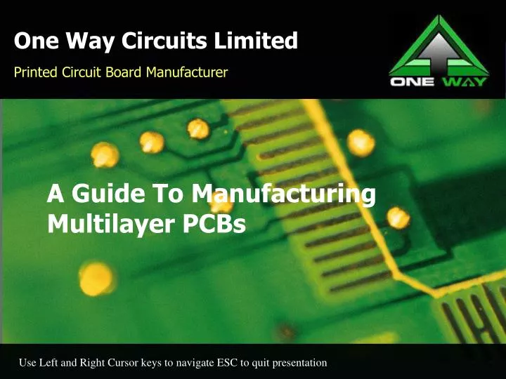
One Way Circuits Limited. Printed Circuit Board Manufacturer. A Guide To Manufacturing Multilayer PCBs. Use Left and Right Cursor keys to navigate ESC to quit presentation. A Guide to Manufacturing Multilayer PCBs. Presentation Title: A Guide to Manufacturer Multilayer PCBs.

E N D
One Way Circuits Limited Printed Circuit Board Manufacturer A Guide To Manufacturing Multilayer PCBs Use Left and Right Cursor keys to navigate ESC to quit presentation
A Guide to Manufacturing Multilayer PCBs • Presentation Title:A Guide to Manufacturer Multilayer PCBs. • Created / Modified:15th September 2009. • Compiled By:One Way Circuits Limited. • Description:The following is a guide only.
Inner layer material is supplied in cut panels. • Inner Layer material is thin pieces of rigid epoxy glass material. Handling precautions are important. • The panels are cleaned ready for the application of an etching Resist film on which the circuit pattern will be printed. INNER LAYERPREPARATION
A light-sensitive etching Resist film is applied. • A Positive inner layer image is printed using a negative artwork. • The light-hardened areas remain intact after developing protecting the base Copper. • The developed resist exposes the base copper which is then is etched. • The etching resist is then removed to reveal the copper image of the inner layer. ETCHING RESIST
Layers Are Exposed to UV Light – Photo Shows Panel after Exposure to Light.
The Layer is Etched Leaving the Circuit Image – the resist protects the Circuit from etching.
The Layer is Stripped of Resist – Leaving the Circuit Image in Copper.
The Copper is chemically treated to ensure good adhesion to the pre-preg that separates the layers. • An Oxide process (or similar) is used to increase the surface roughness of the Copper to aid adhesion. ADHESION PROMOTION
The Copper is chemically treated to ensure good adhesion during bonding.
Inner Layers and Copper foil are interleaved with pre-preg. • Inner Layers are interleaved with pre-preg and copper foil is placed on the outside before bonding together. LAY - UP (4 Layer)
Multi-layer P.C.B’s • Higher complexity requirements have forced the circuit route (tracking) to be passed between several layers of circuitry. Several layers of circuitry have to be bonded together and inter-connected to each other via plated through holes. Buried Via Layer
The layers and foil are then bonded together under heat and pressure. • As the heat is applied the semi - cured resin contained within the pre-preg melts. • Combined with the pressure applied during the bonding process, the resin flows within the layers before finally becoming hard, sealing all materials together as one board. BONDING
Tooling holes are drilled locating off internal targets to ensure accurate drill hole to Innerlayer registration. • The bonded panels are drilled, making sure that the inner layer circuit features are drilled centrally. DRILLING
Electroless copper plating provides the electrical connection between the layers. A thin deposit of Copper on internal walls of holes provides the conductivity for the electroplating processes. ELECTROLESS COPPER
Plating Resist is applied to the panels ready for electroplating. A light-sensitive Resist is applied, to mask parts of the base Copper from being plated. RESIST LAMINATION
Plating Resist is applied to the panels ready for electroplating. • A film-work which has the circuit image in black is applied to the board ready for printing. • High intensity ultra-violet light passes through the clear areas of the film-work this hardens the Resist. PRINTING
A Plating Resist is applied, this is mask that protects areas that do not require plating. U/v light Has hardened the Resist through the clear parts of the Film-work. Non hardened areas of photo Resist Remain Soft and are dissolved Into the developer solution. PLATING RESIST
A plating Resist is applied as a mask to prevent unwanted Copper from becoming plated.
The panels are Electroplated with Copper to form the circuit features. • The drilled holes, already made conductive with Electroless Copper, are plated up to a thickness Suitable for carrying current through the finished board. PATTERN PLATING
Electroplate Tin as an etch Resist. • The Tin plating will protect the Copper plated circuit features against the etching chemicals which will be used to dissolve the unwanted surplus base copper. TIN PLATING
The Photo resist is chemically stripped after plating. • The plating Resist is removed to reveal the now “surplus” base Copper which is removed during the etching process, leaving only the Tin plated circuit features. STRIP PLATING RESIST
Panel After Resist Stripping – Tin Plate acts as an etch Resist.
The exposed Copper is now etched. • The unwanted Copper is now etched away leaving only the circuit features which were protected with Tin. ETCHING
Remove Tin Etch Resist leaving the circuit features in Copper. • Tin plating is stripped from the circuit features. • You can see how the Copper plating through the holes is used to connect the layers together and so form the circuit networks. STRIP TIN
Circuit after Tin Strip now ready for Soldermask Application.
Solder Resist or Solder Mask. • A photo - imageable coating is applied to the circuit. • This inhibits metal finishing or soldering of the covered areas. SOLDER RESIST
Finishing. • A solderable finish is applied to the exposed Copper, followed by: Component identification, Routing, Testing, Final Inspection, Despatch to customer: FINISHING PROCESSES
Board now has Solderable finish and Ident and is ready to cut to size.
Board is Profiled to size – picture shows 2 boards in biscuit frame.
Testing. • Board is then electronically tested to customers data.